Wafer solar cell
a solar cell and wafer technology, applied in the field can solve the problems of increased shading, increased consumption of costly screen printing pastes, and power loss of wafer solar cells
- Summary
- Abstract
- Description
- Claims
- Application Information
AI Technical Summary
Benefits of technology
Problems solved by technology
Method used
Image
Examples
Embodiment Construction
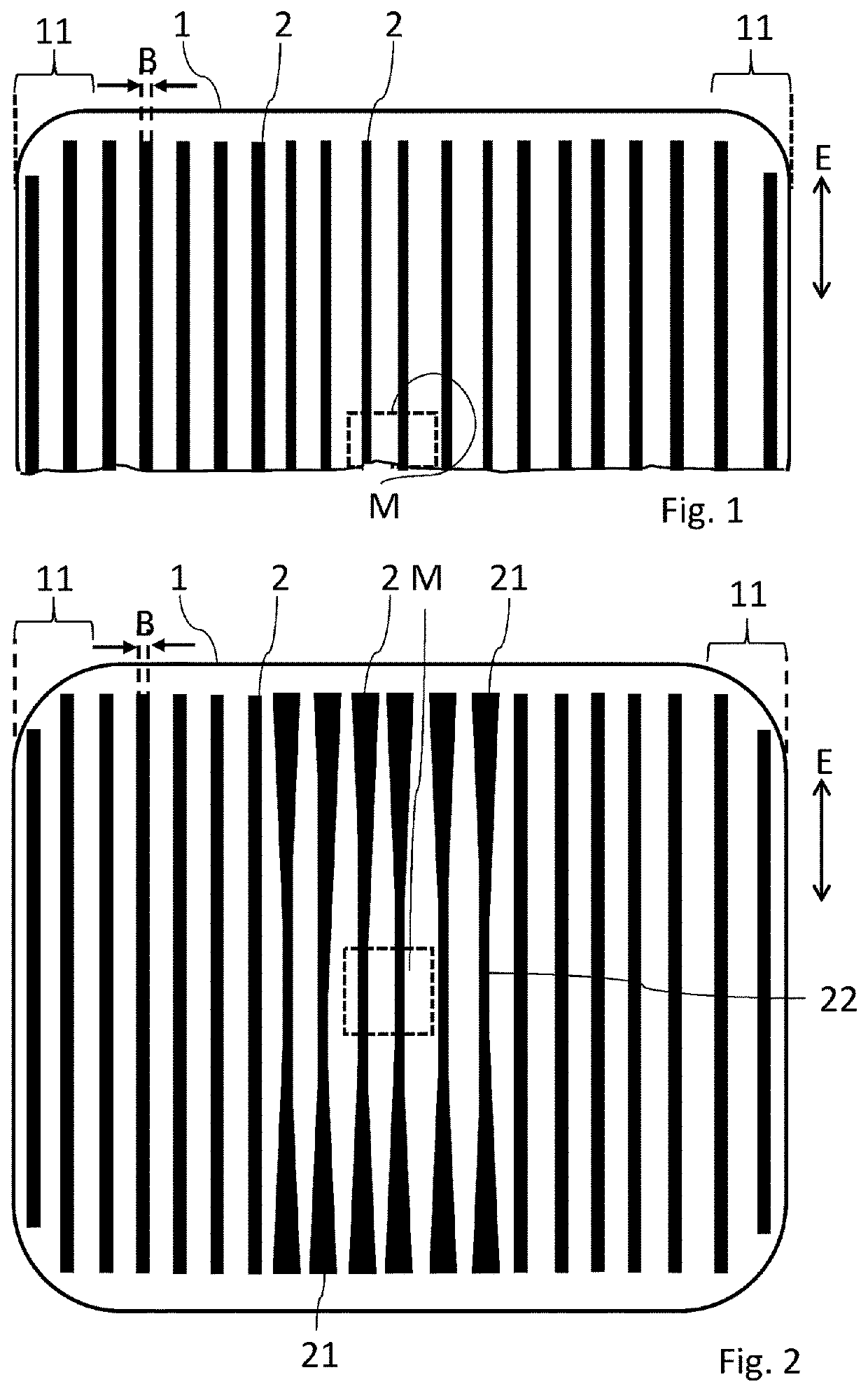
[0035]FIG. 1 shows a partial top view of a wafer solar cell according to the invention. The wafer solar cell has a solar cell surface 1 and a plurality of finger electrodes 2. The finger electrodes 2 are arranged on the solar cell surface 1 and extend in parallel to one another in an extension direction E along the solar cell surface 1. The finger electrodes 2 each have a width B perpendicular to the extension direction E, which is constant in each case along the extension direction E. The respective width B of the finger electrodes 2 increases, starting from a center region M of the solar cell surface 1 viewed transversely to the extension direction E, toward the finger electrodes 2 in edge regions 11 of the solar cell surface 1.
[0036]The center region M is a region which, starting from the center point (not shown) of the solar cell surface 1, occupies 10% of the solar cell width. Each edge region 11 is a region which, starting from an edge (not shown) of the solar cell surface 1, ...
PUM
 Abstract
Description
Claims
Application Information
