

A topological bulk laser and method based on band inversion and reflection of optical field
- Summary
- Abstract
- Description
- Claims
- Application Information
AI Technical Summary
Benefits of technology
Problems solved by technology
Method used
Image

Examples
embodiment 1
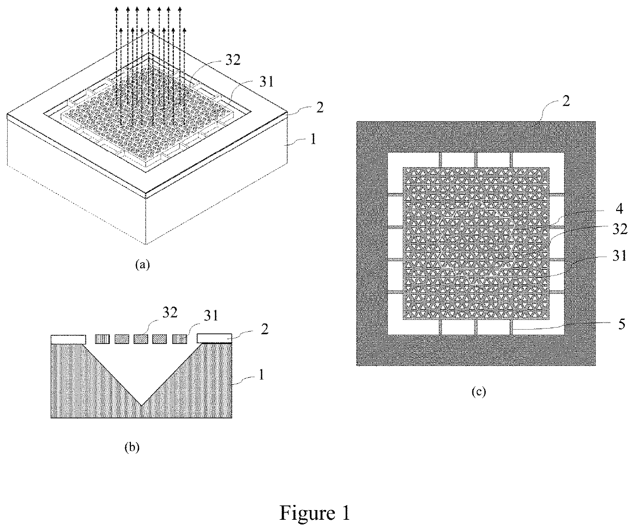
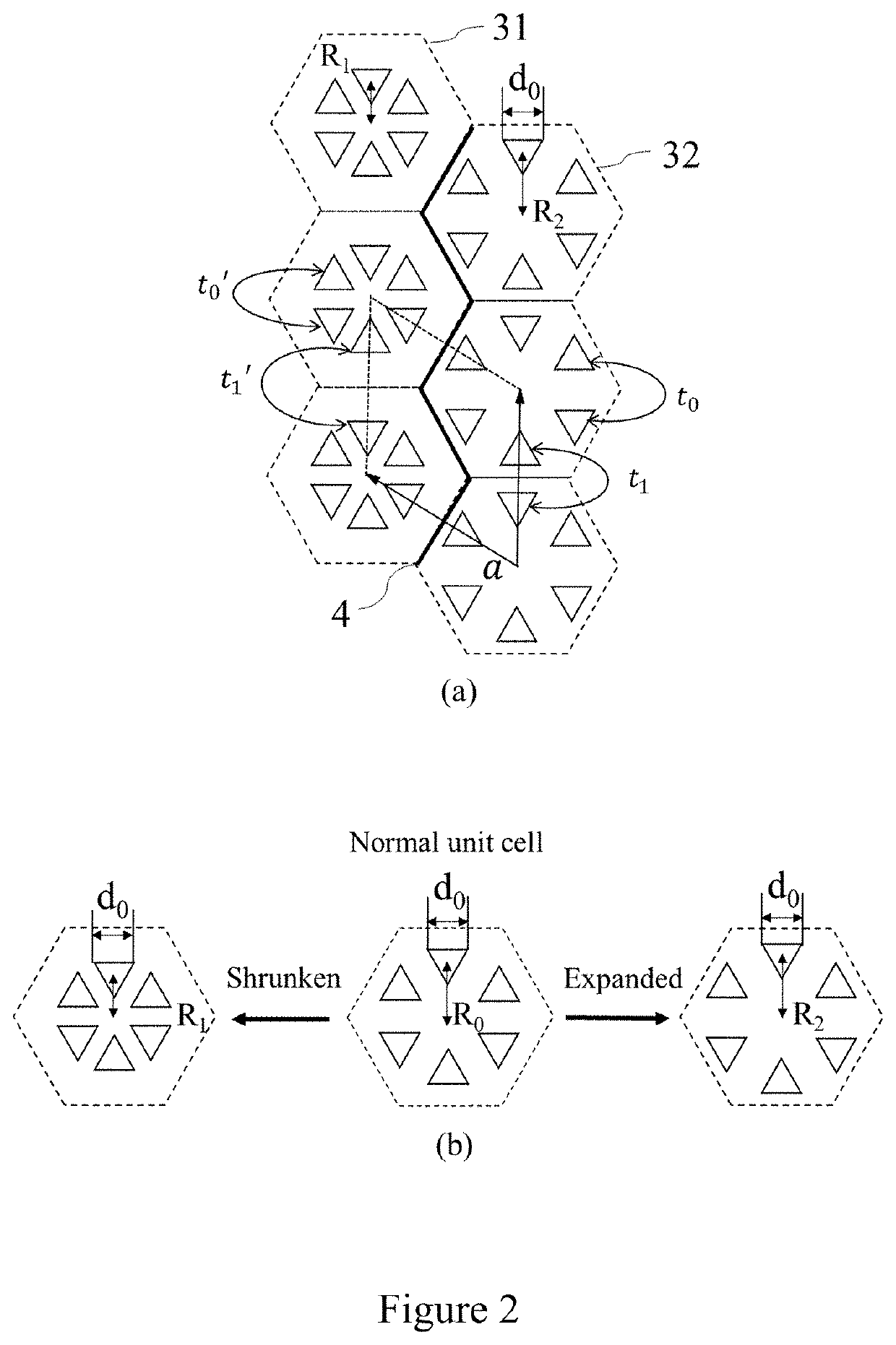
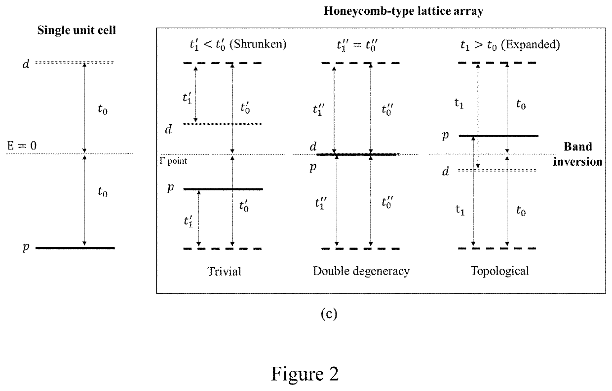
[0043]As shown in FIGS. 1a-1c, this embodiment adopts optical pumping, and the topological bulk laser based on band-inversion-induced reflection consists of topological photonic crystal and topologically trivial photonic crystal using two-dimensional honeycomb-type photonic crystal. By etching the active layer 2, topological photonic crystal and trivial photonic crystals are constructed. The material of the active layer is a multilayer quantum well structure (such as InGaAsP / InGaAs) grown on a semiconductor substrate 1 (such as InP) by epitaxy growth. By changing the elements and element composition of the active material, the refractive index is optional between 2.5-3.5. The trivial photonic crystal 31 and the topological photonic crystal 32 are spliced together as a whole, forming an interface. Bending the interface to a closed contour, it can form a laser cavity inside the interface. When the laser cavity consists of topological photonic crystal, the lasing mode is a quadrupole a...
embodiment 2
[0055]As shown in FIG. 12, this embodiment adopts an electrically injected surface-emitting topological bulk laser. Take the design method of the topological bulk laser based on band inversion induced reflection in Embodiment 1 to the electrical injection material systems, a practical electrically injected surface-emitting laser with controllable size, high directionality, low threshold, narrow linewidth, and high side-mode suppression ratio can be obtained.
[0056]The structure of this device includes a semiconductor epitaxial layer which consists of an N-type substrate 6, an N-type contact layer 7 located on the N-type substrate, N-type confinement layer 8, active layer 2 located on the N-type confinement layer, P-type confinement layer 9 located on the active layer, P-type contact layer 10 located on the P-type confinement layer. The refractive index of the N-type and P-type material is slightly smaller than that of the active layer, and the refractive index difference is optional ...
PUM
 Abstract
Description
Claims
Application Information