Nonvolatile memory with reduced write time/write verify time and semiconductor device thereof

a non-volatile memory, write verification technology, applied in static storage, digital storage, instruments, etc., can solve the problems of flash memory 1 defective, and it takes a long total time for a large capacity memory to achieve data wri

Inactive Publication Date: 2000-01-04
RENESAS ELECTRONICS CORP
View PDF2 Cites 39 Cited by
  • Summary
  • Abstract
  • Description
  • Claims
  • Application Information

AI Technical Summary

Problems solved by technology

If a particular number of times of rewriting cannot achieve correct writing, a decision is made that the flash memory 1 is defective.
With such an arrangement, the conventional involatile memory has a problem in that the data write time is basically determined by the bus width of the data port 5, and hence it takes a long total time for a today's large capacity memory to achieve the data write.

Method used


Image

  • Nonvolatile memory with reduced write time/write verify time and semiconductor device thereof
  • Nonvolatile memory with reduced write time/write verify time and semiconductor device thereof
  • Nonvolatile memory with reduced write time/write verify time and semiconductor device thereof

Examples


embodiment 1

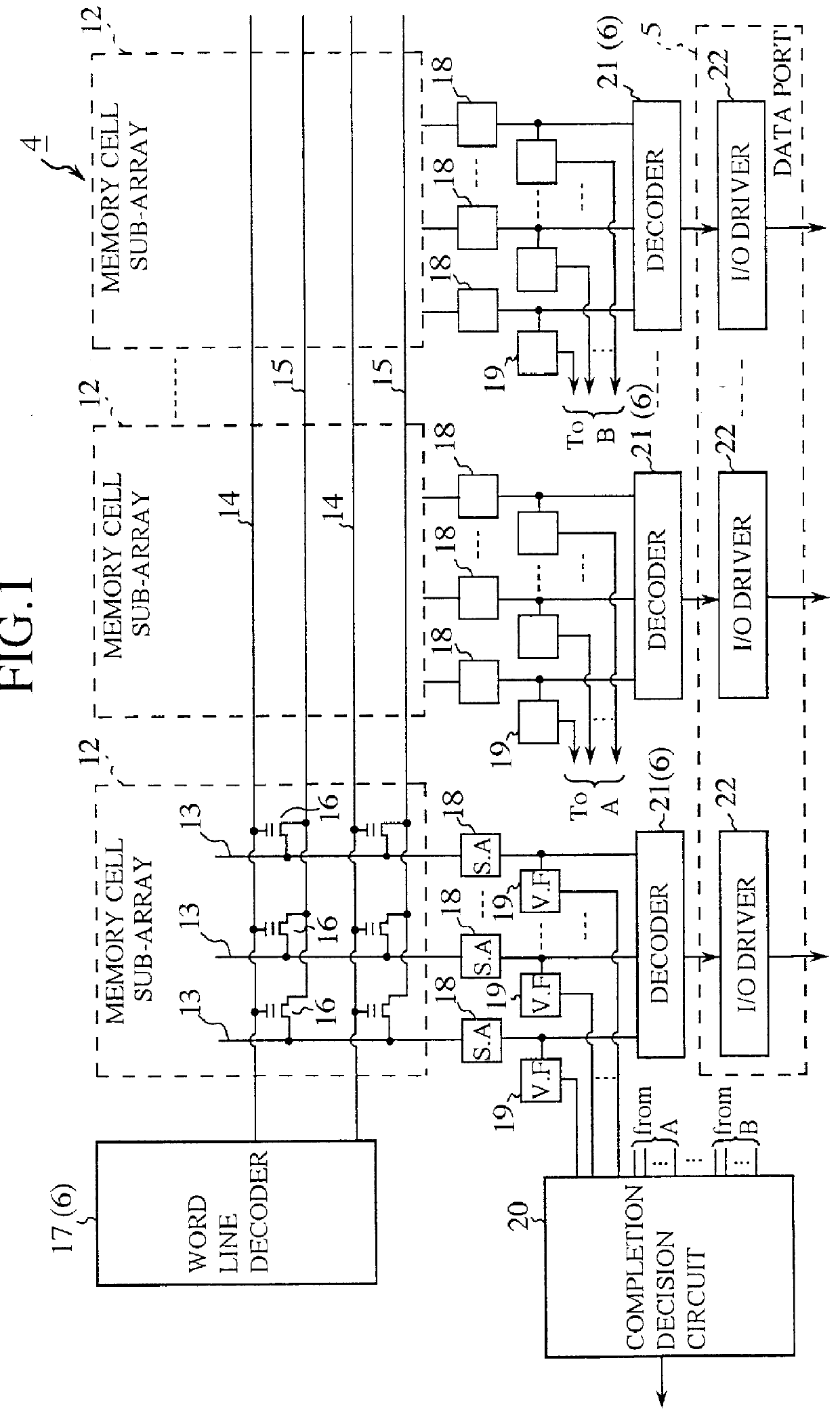
FIG. 1 is a block diagram showing a flash memory in accordance with the present embodiment. In FIG. 1, the reference numeral 5 designates a data port connected to an external data bus; and reference numerals 22s each designate an I / O driver connected to one of the bus lines of the external data bus. The total number of the I / O drivers 22 are P, where P is an integer equal to or greater than one. Reference numerals 16s each designate a memory transistor; 12s each designate a memory cell sub-array consisting of M.times.N memory transistors 16 corresponding to each I / O driver 22, where M and N are each an integer equal to or greater than one; and 13s each designate a bit line, where each memory cell sub-array 12 includes M bit lines 13. Reference numerals 21s each designates a decoder provided for each memory cell sub-array 12 for selecting one of the M bit lines 13 to be connected to the I / O driver 22. The reference numeral 17 designates a word line decoder for selecting the memory tr...

embodiment 2

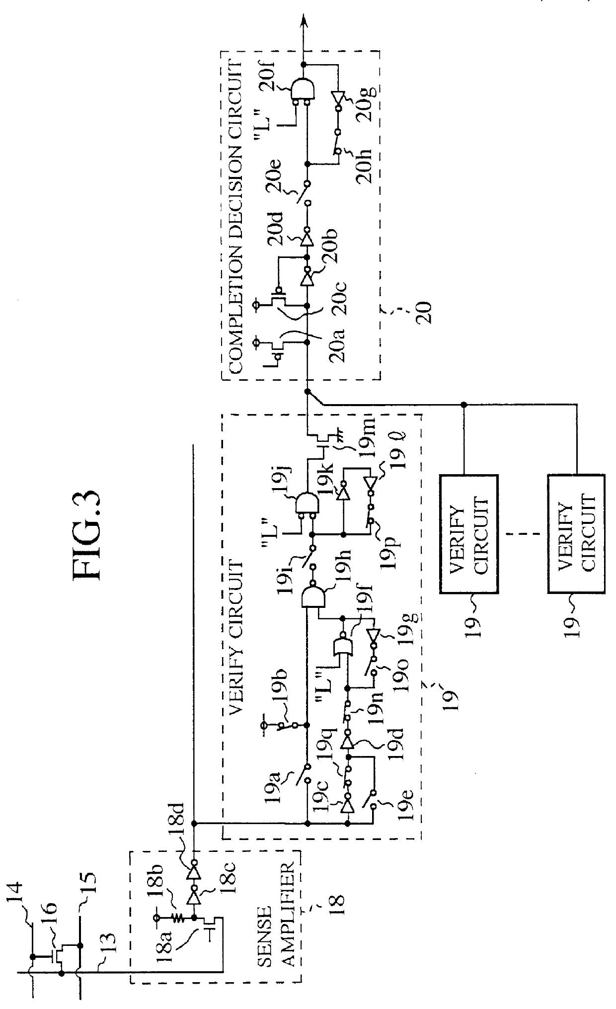
FIG. 3 is a circuit diagram showing a configuration from the bit line 13 to the completion decision circuit 20 in an embodiment 2 of the flash memory in accordance with the present invention. In FIG. 3, the reference numeral 18a designates a select transistor having its source connected to the bit line 13 and its gate supplied with a high level select signal when data is read through the bit line 13; 18b designates a sense amplifier pullup resistor connected between the drain of the select transistor 18a and a high potential power supply; and 18c and 18d each designate an inverter for amplifying the drain voltage to be output.

Reference numerals 19a and 19e each designate a verify switch which is open during the erase verify check process and is closed during the write verify check; 19b and 19q each designate a verify switch that is closed during the erase verify check process and is open during the write verify check; 19c and 19d each designate an inverter for inverting the output l...

embodiment 3

FIG. 4 is a block diagram showing an embodiment 3 of the flash memory in accordance with the present invention. In FIG. 4, reference numerals 23s each designate a first decoder connected with a plurality of bit lines 13 for selecting one of them; and 24s each designate a second decoder connected with the outputs of a plurality of first decoders 23 for selecting one of them. The sense amplifiers 18 are provided in one-to-one correspondence with the first decoders 23, and connected between the first decoders 23 and the second decoder 24. Reference numerals 31s each designate a page data latch that is provided for each bit line 13, and stores data to be written to the bit line 13. Since the remaining portion is the same as that of the embodiment 2, description thereof will be omitted by designating the like portions by the same reference numerals.

Next, the operation of the present embodiment 3 will be described.

In the data write process, the data is continuously and sequentially writte...


PUM


Abstract

An involatile memory which carries out, in a flash memory itself, verify check of the flash memory for respective bit lines, and produces an overall verify check result from a completion decision circuit to a tester. This makes it possible to solve a problem of a conventional flash memory in that the time taken by the verify check depends on the bus width of an external data bus, because it carries out the verify check by reading data from the flash memory through the external bus. Thus, the time taken by the verify check can be reduced.

Description

1. Field of the InventionThe present invention relates to a nonvolatile memory such as a flash memory including memory transistors each having a floating gate, and more particularly to an improvement in the memory to reduce the time needed for writing data into the memory transistors.2. Description of Related ArtFIG. 7 is a block diagram showing a conventional flash memory and a configuration for writing data into it. In FIG. 7, the reference numeral 1 designates a flash memory; 2 designates a tester for writing data into the flash memory 1; and 3 designates an external data bus for interconnecting them. The reference numeral 4 designates a memory cell array including a plurality of memory transistors; 5 designates a data port for interconnecting the memory cell array 4 with the external data bus 3; and 6 designates an address input port for selecting from the memory cell array 4 memory transistors to be connected to the data port 5. The reference numeral 7 designates a tester side ...

Claims


Application Information

Patent Timeline
Patent Type & Authority Patents(United States)
IPC IPC(8): G11C16/06G11C16/34G11C29/50G11C29/04G11C16/02
CPCG11C16/3454G11C16/3459G11C29/50G11C16/04G11C16/00
Inventor TANAKA, NOBUHIKO
Owner RENESAS ELECTRONICS CORP
Why Eureka
Try Eureka