

Lithographic mask and method for fabrication thereof
a technology of lithographic masks and masks, applied in the field of improving the resolution of electronic masks, can solve the problems of increasing the proximity effect, reducing the resolution, and reducing the accuracy of the mask, so as to reduce the detrimental reduce the proximity effect of electronic circuits, and reduce the effect of backscattered electrons
- Summary
- Abstract
- Description
- Claims
- Application Information
AI Technical Summary
Benefits of technology
Problems solved by technology
Method used
Image

Examples
Embodiment Construction
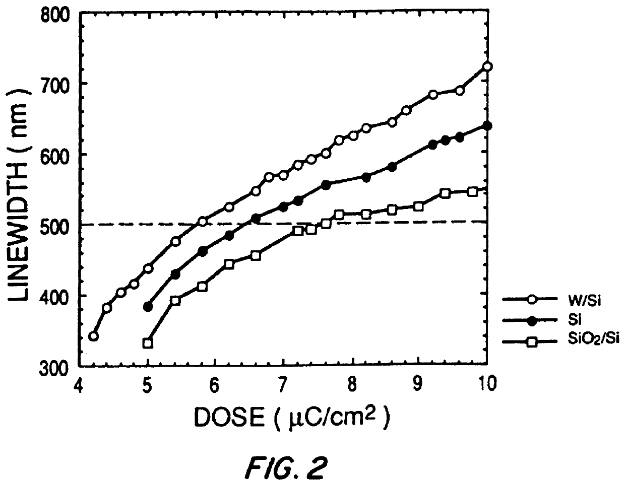
This invention generally relates to improving resolution in electronic masks made by high voltage electron beam lithography by reducing proximity effects. More specifically, this invention relates to interposition of a dielectric layer between a resist and an absorber disposed on a transparent support.
FIG. 1 more specifically illustrates the invention herein which comprises transparent support 18 having disposed directly thereover and being in contact with absorber 20, dielectric layer or film 22 disposed over and being in contact with absorber 20, and a suitable resist layer 24 disposed directly over and being in contact with dielectric layer 22. High voltage or high energy beam 26 is directed at the resist layer 24 from above.
The purpose of the dielectric layer is to improve resolution of electronic circuits which are made using the masks. In high voltage electron beam direct write lithography, the electrons which are backscattered from the absorber create fast secondary and secon...
PUM
 Abstract
Description
Claims
Application Information