Ultrasonic photoresist process monitor and method

Inactive Publication Date: 2000-02-22
THE BOARD OF TRUSTEES OF THE LELAND STANFORD JUNIOR UNIV
View PDF10 Cites 18 Cited by
  • Summary
  • Abstract
  • Description
  • Claims
  • Application Information

AI Technical Summary

Benefits of technology

It is a further object of the present invention to provide a photoresist proce

Problems solved by technology

If the solvent is not fully evaporated or if the prebake time is too long,

Method used


Image

  • Ultrasonic photoresist process monitor and method
  • Ultrasonic photoresist process monitor and method
  • Ultrasonic photoresist process monitor and method

Examples


Embodiment Construction

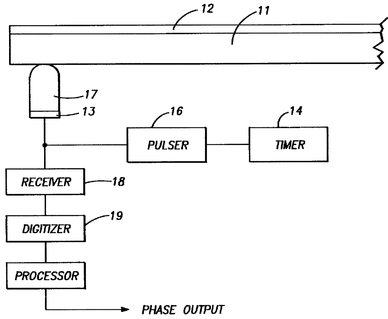
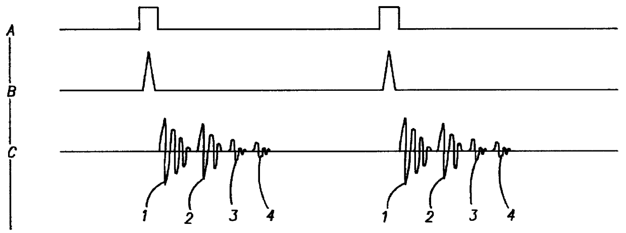
In FIG. 1 a wafer 11 is shown with a photoresist film 12. Ultrasonic waves are used to determine changes in the photoresist film during the prebake process. The ultrasonic waves or pulses are generated by a piezoelectric transducer 13. High voltage pulses are applied across zinc oxide piezoelectric transducer 13 which in this example resonates at 260 MHz. The resonant frequency is determined by the thickness of the transducer. The transducer causes mechanical displacement which launches longitudinal acoustic waves. A timer 14 applies timing pulses (FIG. 3A) to a purser 16. The pulser 16 applies the high voltage pulses (FIG. 3B) across the piezoelectric transducer 13.

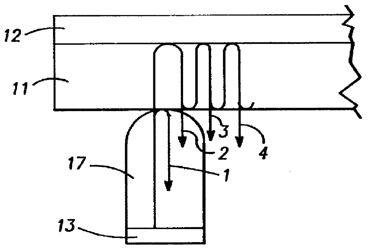
The longitudinal waves excited by the transducer are coupled into the underside of the wafer by direct contact through a sapphire buffer rod 17. These waves are reflected from the silicon / photoresist interface and from the buffer rod wafer interface. The reflection of the pulses directly from this buffer rod wafer interf...


PUM


Abstract

There is provided a monitor and method for monitoring the condition of a photoresist film on a wafer during baking in which the phase of high frequency ultrasonic pulses reflected from the wafer/photoresist interface provides an indication of the condition of the photoresist film.

Description

The present invention relates generally to an ultrasonic photoresist process monitor and method and more particularly to an in situ monitor which monitors the prebaking and baking photoresist film processing.In the manufacture of integrated circuits the various circuit components are defined by using a photoresist layer which is applied to the surface of a semiconductor wafer, exposed and developed. The photoresist is applied to the surface of the wafer by applying a few drops of liquid resist onto a spinning wafer to obtain a photoresist film of predetermined thickness. The photoresist liquid film is prebaked to remove any excess solvent that is initially added to the resist as well as to anneal the polymer film, allowing the resin molecules to relax into their lowest energy state. This thin film of resist is typically on the order of 1-2 .mu.m thick. The film thickness changes about 0.5 .mu.m during prebake.If the solvent is not fully evaporated or if the prebake time is too long,...

Claims


Application Information

Patent Timeline
IPC IPC(8): G01N29/44G01N29/46G01N29/07G01N29/04
CPCG01N29/07G01N29/075G01N29/46G01N2291/011G01N2291/014G01N2291/0237G01N2291/02881G01N2291/0421G01N2291/044G01N2291/048
Inventor KHURI-YAKUB, BUHRUS T.MORTON, SUSANDEGERTEKIN, F. LEVENT
Owner THE BOARD OF TRUSTEES OF THE LELAND STANFORD JUNIOR UNIV
Why Eureka
Try Eureka