Two square NVRAM cell

a non-volatile random access memory, two-square technology, applied in the direction of electrical equipment, semiconductor devices, instruments, etc., can solve the problem that memory designers have not achieved a state of the art unit cell that is smaller than 6-8 squares

Inactive Publication Date: 2000-03-21
INT BUSINESS MASCH CORP
View PDF7 Cites 66 Cited by
  • Summary
  • Abstract
  • Description
  • Claims
  • Application Information

AI Technical Summary

Problems solved by technology

However, memory designers have not achieved a state of the art unit cell that is smaller than 6-8 squares, where a square is the smallest unit design area for a given technology, e.g., 0.2 .mu.m.times.0.2 .mu.m.

Method used


Image

  • Two square NVRAM cell
  • Two square NVRAM cell
  • Two square NVRAM cell

Examples


Embodiment Construction

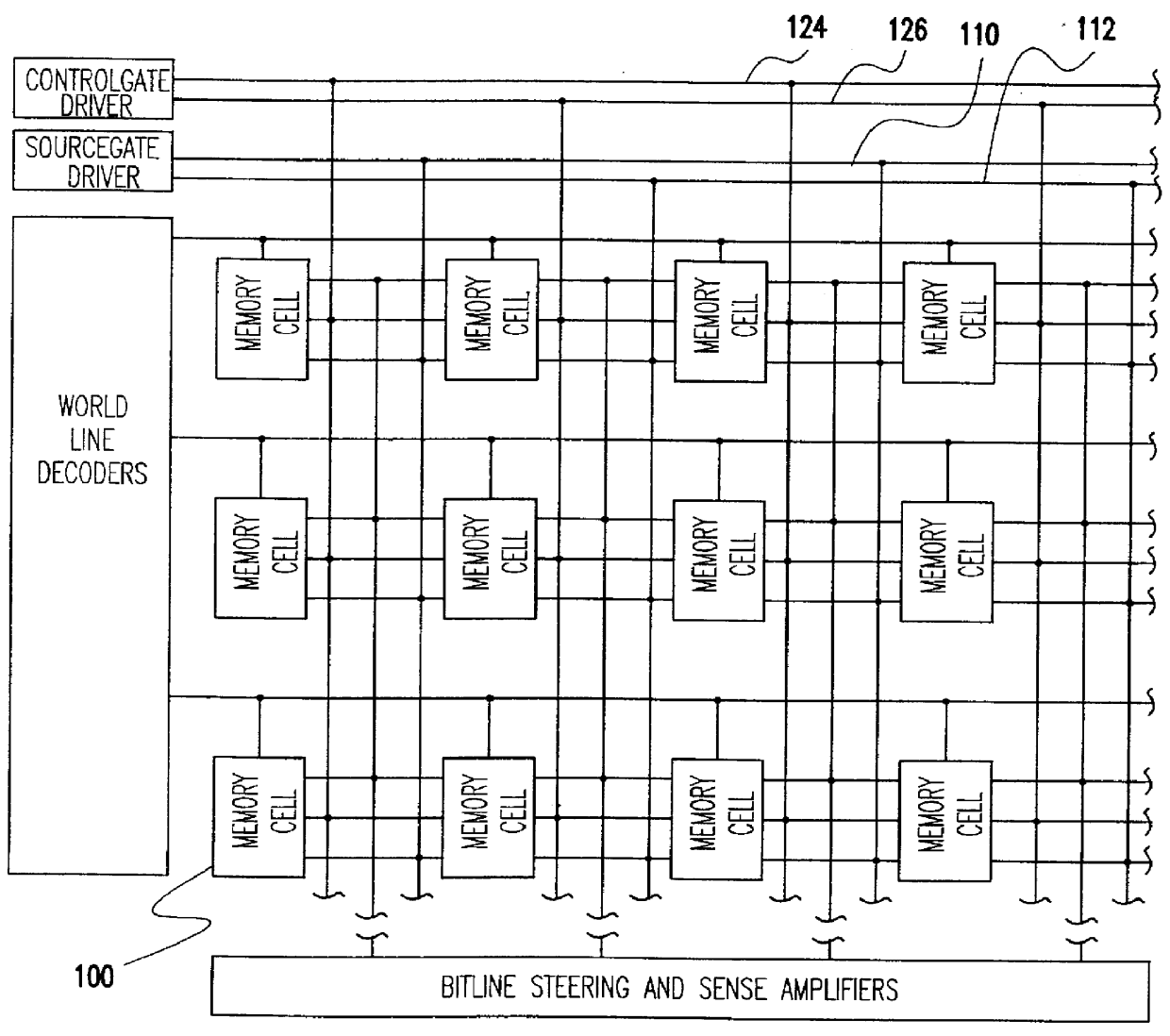
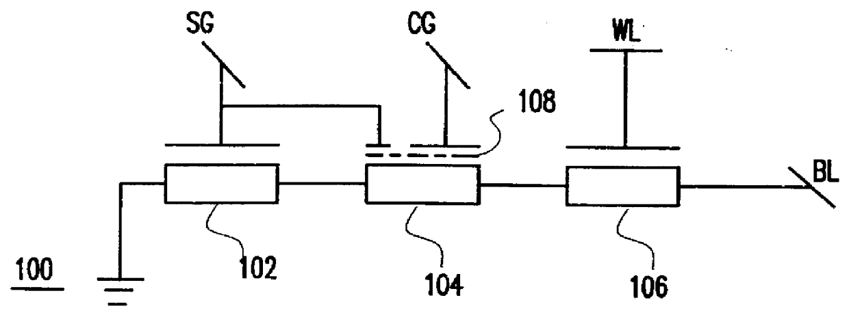
Referring now to the drawings, and more particularly to FIG. 1A which shows a schematic of a preferred non-volatile random access memory (NVRAM) cell 100. Three FETs 102, 104 and 106 are stacked in a NAND-like structure. Source device 102, which is connected between ground and floating gate device 104, has its gate tied to a source gate (SG) line. Word line select device 106 is connected between a bit line (BL) and floating gate device 104 and has its gate tied to a passing word line (WL). Control gate (CG) line and SG are capacitively coupled to the floating gate (represented by dashed line 108) of each floating gate device 104.

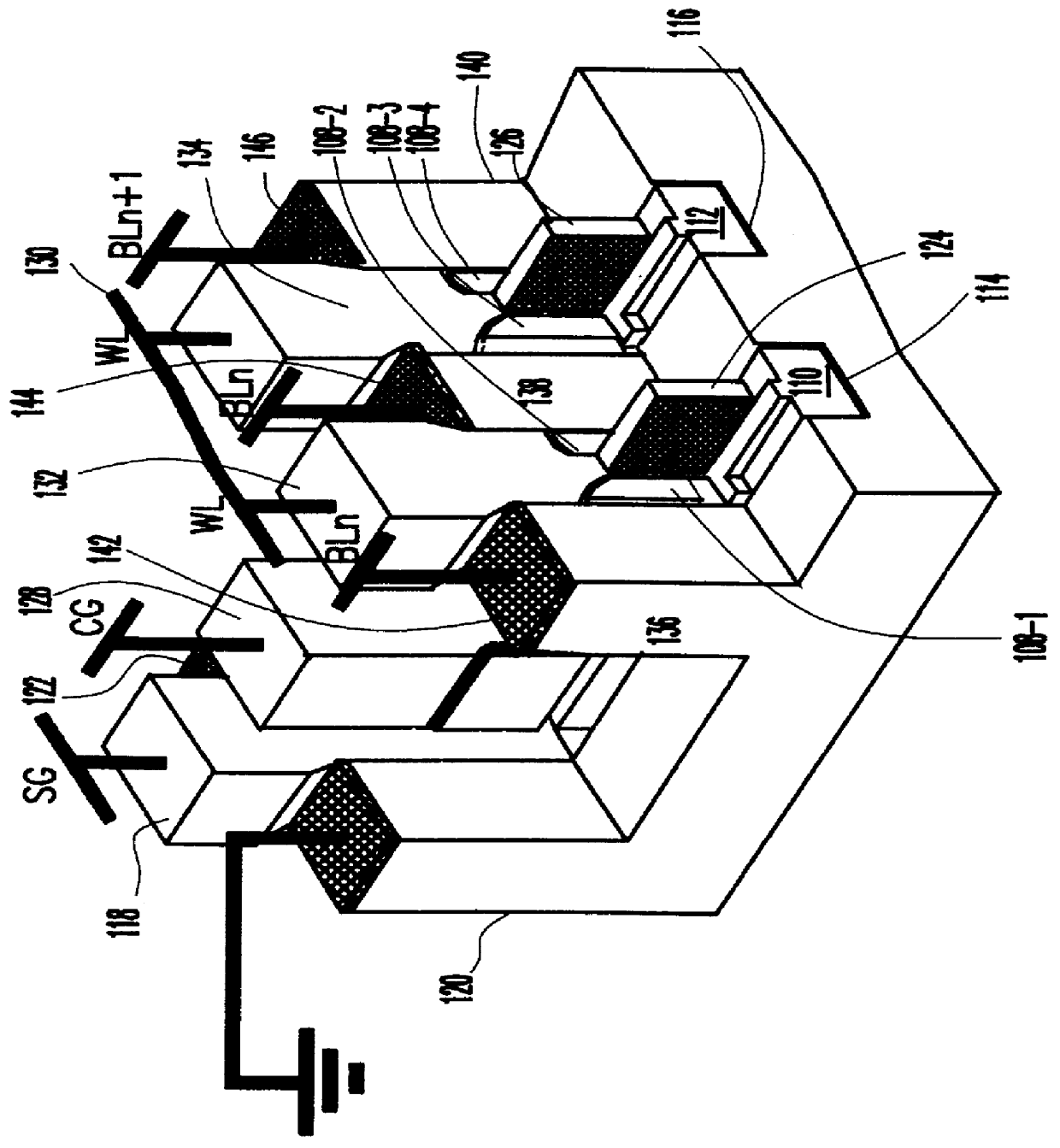
As can be seen from FIG. 1B, which is a cross-sectional view of a portion of a preferred embodiment array, unlike prior art NVRAM cells, adjacent pairs of preferred NVRAM cells 100 share a common wordline (WL) and a common bitline (BL). In FIG. 1B, source gate lines 110 and 112 each extend along the bottom of a trench 114 and 116, respectively. Each source g...


PUM


Abstract

A non-volatile random access memory (NVRAM) cell and method of fabrication thereof. Pairs of NVRAM cells, each including three FETs stacked in a NAND-like structure are formed vertically in silicon pillars. Source devices at the bottom of the pillar selectively provide ground to one of the cells. A floating gate extends upward from the source device's gate line. A control gate plate extending between adjacent pillars selectively provides a programming voltage to the control gate. Both the source gate and the control gate are capacitively coupled through silicon rich oxide to the floating gate. Polysilicon plugs between silicon pillars are word line gates for cells in adjacent pillars. A diffusion at the top of each pillar is a bit line contact for both cells at the pillar. Each pair of cells on a pillar are on a common bit line and a common word line. The word line, control gate and source gate line select individual cells in the pair.

Description

1. Field of the InventionThe present invention generally relates to non-volatile memory cells and more particularly to a three-dimensional, direct-write non-volatile random access memory (NVRAM) cell having a high integration density and methods fabrication therefor.2. Background DescriptionNon-volatile floating gate memory cells, such as in a non-volatile random access memory (NVRAM) arrays are well known in the industry. In NVRAM cells, the cell's conductive state is determined by the charge state of the cell's floating gate. The floating gate is an electrically isolated gate of a field effect transistor (FET) stacked in a two device NAND-like structure. Charge is forced onto or removed from the floating gate through a thin insulator layer that, normally (during a read operation), isolates the gate electrically from other adjoining conductive layers. Typically, a negatively charged floating gate is representative of a binary one state, while an uncharged floating gate is represent...

Claims


Application Information

Patent Timeline
Patent Type & Authority Patents(United States)
IPC IPC(8): H01L21/70G11C16/04H01L27/115H01L21/8247
CPCG11C16/0433H01L27/115H01L27/11556H10B69/00H10B41/27
Inventor LAM, CHUNG H.
Owner INT BUSINESS MASCH CORP
Why Eureka
Try Eureka