

Planar channel-type MOS transistor
a transistor and planar channel technology, applied in the field of semiconductor devices, can solve the problems of non-stable semiconductor devices, difficult to realize the reduction of difficulty in reducing the size of individual elements or reducing the total number of necessary process steps
- Summary
- Abstract
- Description
- Claims
- Application Information
AI Technical Summary
Problems solved by technology
Method used
Image

Examples
Embodiment Construction
The principles of the present invention are particularly useful when applied to a semiconductor device, particularly a planar channel-type MOS transistor, and a fabrication process therefor, an embodiment of which will now be described in detail with reference to the accompanying drawings.
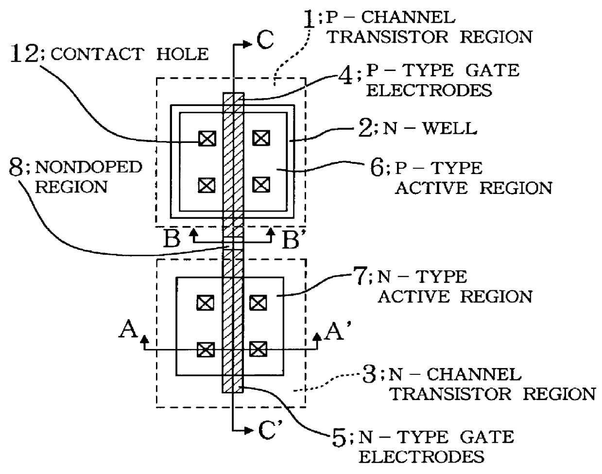
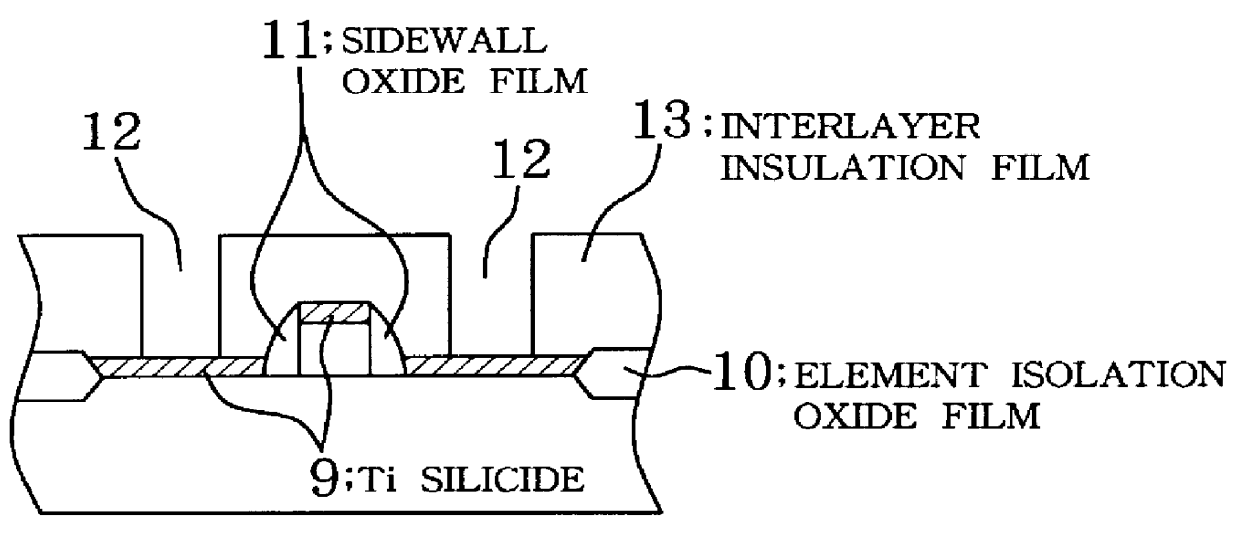
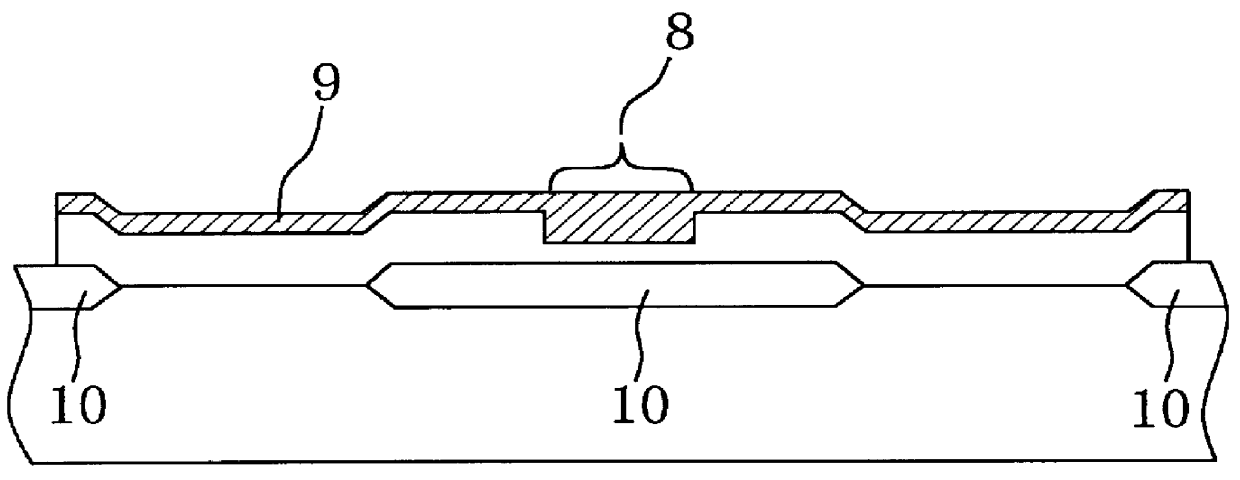
In FIG. 1(a), one rectangle (top) indicated by dashed lines defines a p-channel transistor region 1 in which an n-well 2 is formed in a predetermined region of a p-type semiconductor substrate and in which element forming regions are located as a p-type active region 6 and a p-type gate electrode 4. Another rectangle (bottom) indicated by dashed lines in FIG. 1(a) defines an n-channel transistor region 3 which occupies a p-type substrate region adjacent to the p-channel transistor region 1 and in which element forming regions are located as an n-type active region 7 and an n-type gate electrode 5. Reference number 12 designates a contact hole and reference number 13 designates an interlayer insulat...
PUM
 Abstract
Description
Claims
Application Information