Mixed-crystal-face strain-Si vertical-channel CMOS (complementary metal oxide semiconductor) integrated device and preparation method

A technology of vertical channels and mixed crystal planes, applied in semiconductor/solid-state device manufacturing, electric solid-state devices, semiconductor devices, etc. The effect of the process steps

Inactive Publication Date: 2015-07-01
XIDIAN UNIV
View PDF2 Cites 0 Cited by
  • Summary
  • Abstract
  • Description
  • Claims
  • Application Information

AI Technical Summary

Problems solved by technology

At the same time, NMOS and PMOS are prepared on the same crystal plane, and their mobility cannot be optimal at the same time

Method used


Image

  • Mixed-crystal-face strain-Si vertical-channel CMOS (complementary metal oxide semiconductor) integrated device and preparation method
  • Mixed-crystal-face strain-Si vertical-channel CMOS (complementary metal oxide semiconductor) integrated device and preparation method
  • Mixed-crystal-face strain-Si vertical-channel CMOS (complementary metal oxide semiconductor) integrated device and preparation method

Examples


Embodiment 1

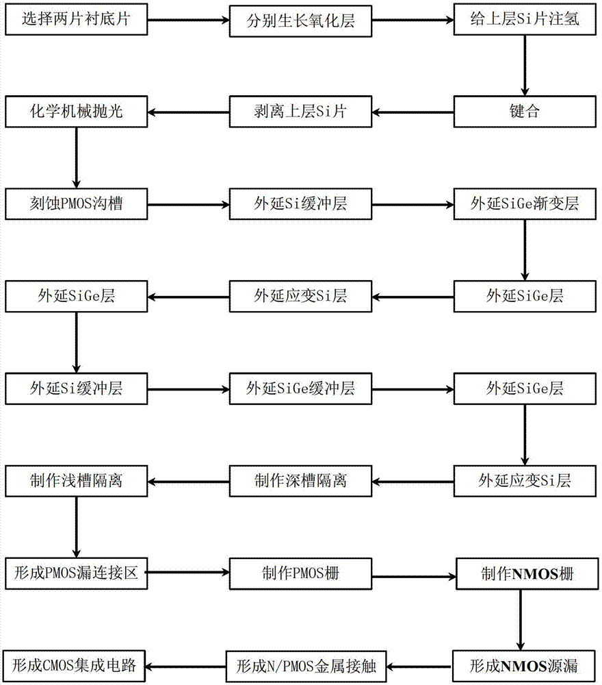
[0062] Embodiment 1: Prepare 22nm mixed crystal plane strained Si vertical channel CMOS integrated device and circuit, the specific steps are as follows:

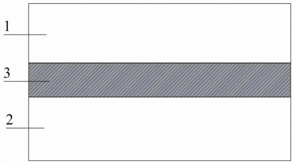
[0063] Step 1, SOI substrate material preparation, such as figure 2 , image 3 shown.

[0064] (1a) Select the N-type doping concentration as 1×10 15 cm -3 Si sheet 1 with a crystal plane of (100) is oxidized on the surface, and the thickness of the oxide layer is 0.5 μm, which is used as the upper substrate material, and hydrogen is injected into the substrate material;

[0065] (1b) Select the N-type doping concentration as 1×10 15 cm -3 The Si sheet 2 with a crystal plane of (110) is oxidized on its surface, and the thickness of the oxide layer is 0.5 μm, which is used as the base material of the lower layer;

[0066] (1c) Using a chemical mechanical polishing (CMP) process to polish the surface of the lower and upper substrate materials respectively;

[0067] (1d) The oxide layer 3 on the surface of the polished...

Embodiment 2

[0114] Embodiment 2: Prepare 30nm mixed crystal plane strained Si vertical channel CMOS integrated device and circuit, the specific steps are as follows:

[0115] Step 1, SOI substrate material preparation, such as figure 2 , image 3 shown.

[0116] (1a) Select the N-type doping concentration as 3×10 15 cm -3 The Si sheet 1 with a crystal plane of (100) is oxidized on the surface, and the thickness of the oxide layer is 0.75 μm, which is used as the upper substrate material, and hydrogen is injected into the substrate material;

[0117] (1b) Select the N-type doping concentration as 3×10 15 cm -3 The Si sheet 2 with a crystal plane of (110) is oxidized on its surface, and the thickness of the oxide layer is 0.75 μm, which is used as the base material of the lower layer;

[0118] (1c) Using a chemical mechanical polishing (CMP) process to polish the surface of the lower and upper substrate materials respectively;

[0119] (1d) The oxide layer 3 on the surface of the po...

Embodiment 3

[0166] Embodiment 3: Prepare 45nm mixed crystal plane strained Si vertical channel CMOS integrated device and circuit, the specific steps are as follows:

[0167] Step 1, SOI substrate material preparation, such as figure 2 , image 3 shown.

[0168] (1a) Select the N-type doping concentration as 5×10 15 cm -3 The Si sheet 1 with a crystal plane of (100) is oxidized on the surface, and the thickness of the oxide layer is 1 μm, which is used as the upper substrate material, and hydrogen is injected into the substrate material;

[0169] (1b) Select the N-type doping concentration as 5×10 15 cm -3 The Si sheet 2 with a crystal plane of (110) is oxidized on its surface, and the thickness of the oxide layer is 1 μm, which is used as the base material of the lower layer;

[0170] (1c) Using a chemical mechanical polishing (CMP) process to polish the surface of the lower and upper substrate materials respectively;

[0171] (1d) The oxide layer 3 on the surface of the polished...


PUM

PropertyMeasurementUnit
thicknessaaaaaaaaaa
thicknessaaaaaaaaaa
thicknessaaaaaaaaaa

Abstract

The invention discloses a mixed-crystal-face strain-Si vertical-channel CMOS (complementary metal oxide semiconductor) integrated device and a preparation method. The preparation method includes: preparing an SOI (silicon on insulator) substrate, wherein an upper substrate is a crystal face (100) and a lower substrate is a crystal face (110); etching a deep trench in a PMOS (P-channel metal oxide semiconductor) active region at the temperature of 600-800 DEG C, selectively growing a strain Si PMOS active layer on a multi-layer structure of the crystal face (110), and preparing a compression strain PMOS of a vertical channel on the active layer; and etching a deep trench on an NMOS (N-channel metal oxide semiconductor) active region, selectively growing a strain Si NMOS active layer on a multi-layer structure of the crystal face (100), preparing a tensile strain NMOS of a planar channel on an epitaxial layer, and forming a mixed-crystal-face strain-Si CMOS integrated circuit with a conducting channel of 22-45nm. By the mixed-crystal-face strain-Si vertical-channel CMOS integrated device and the preparation method, the characteristics that migration rate of strain Si materials is higher than that of Si materials and the strain and the migration rate of the strain Si materials are anisotropic are fully used, and the mixed-crystal-face strain-Si CMOS integrated device and the mixed-crystal-face strain-Si CMOS integrated circuit which are excellent in performance are prepared on the basis of the SOI substrate.

Description

technical field [0001] The invention belongs to the technical field of semiconductor integrated circuits, and in particular relates to a mixed crystal plane strained Si vertical channel CMOS integrated device and a preparation method. Background technique [0002] In the contemporary era of highly developed information technology, microelectronic technology represented by integrated circuits is the key to information technology. As the fastest-growing, most influential and most widely used technology in human history, integrated circuits have become an important symbol to measure a country's scientific and technological level, comprehensive national strength and national defense strength. The number of integrated circuits in the whole system is a direct characterization of the advanced nature of the system. [0003] "Moore's Law", which has had a huge impact on the development of the semiconductor industry, states that the number of transistors on an integrated circuit chip...

Claims


Application Information

Patent Timeline
Patent Type & Authority Patents(China)
IPC IPC(8): H01L27/12H01L21/84
Inventor 张鹤鸣李妤晨胡辉勇宋建军宣荣喜王斌王海栋郝跃
Owner XIDIAN UNIV
Why Eureka
Try Eureka