
Damascene NVRAM cell and method of manufacture

Inactive Publication Date: 2000-05-09
IBM CORP
View PDF17 Cites 29 Cited by
  • Summary
  • Abstract
  • Description
  • Claims
  • Application Information

AI Technical Summary

Benefits of technology

It is another object of the invention to provide an NVRAM cell structure which can be formed with fewer, less critical and more economical process steps while increasing manufacturing yield.
It is a further object of the invention to avoid severe interpoly insulator and control gate topography in NVRAM cells which may be integrated at high density in a manner compatible with the inclusion of other devices on the same chip without significant increase of process complexity.
It is yet another object of the invention to provide a process of manufacture which provides substantial flexibility in dopant implantation processes for both memory cells and transistors made by compatible processes, particularly allowing independence of source / drain doping and channel doping.

Problems solved by technology

Nevertheless, delays may be encountered when data required by the processor is not present in the cache, reducing predictability of task completion time.
Further, use of a cache does not provide freedom from other characteristics of the storage medium utilized such as the mechanical vulnerability of magnetic disk drives to wear, impact, vibration and the like.
Each tunnelling operation, however, causes a finite amount of damage to the dielectric and the number of write and erase cycles which can be performed before failure has been limited.
The structure of a NVRAM cell is relatively complex and critical and development of high manufacturing yields consistent with high integration density has proven difficult.
Tunnelling effects on which NVRAMs continue to rely for write and erase operations, however, requires a higher voltage than is required for read operations while high integration density requires small sizes of the memory cells.
Since the control gate must extend over the floating gate where the floating gate, in turn, extends over an isolation structure, severe large step topography is unavoidable in the control gate and the interpoly oxide, as well.
Breaks in the control gate silicide severely compromise manufacturing yield since a control gate generally overlies and provides access to a plurality of NVRAM cells and a break thus isolates and prevents access to cells beyond the break in the control gate.
Accordingly, some degree of compromise of manufacturing yield, integration density and design optimization has been tolerated in previous designs which has increased the cost and limited production and application of high density NVRAMs both at the package level and in various computers and other electronic apparatus.
However, at the present state of the art, due to difficulties with trench filling, throughput of planarization processes and the like, damascene processes are generally limited to the formation of conductors in which the advantages of robustness and fine pitch are pronounced and not otherwise obtainable.
Damascene processes are not widely used for device (e.g. transistors and capacitors) construction within a substrate or layer or with materials which do not reliably fill high aspect ratio grooves or recesses.

Method used


Image

  • Damascene NVRAM cell and method of manufacture
  • Damascene NVRAM cell and method of manufacture
  • Damascene NVRAM cell and method of manufacture

Examples


Embodiment Construction

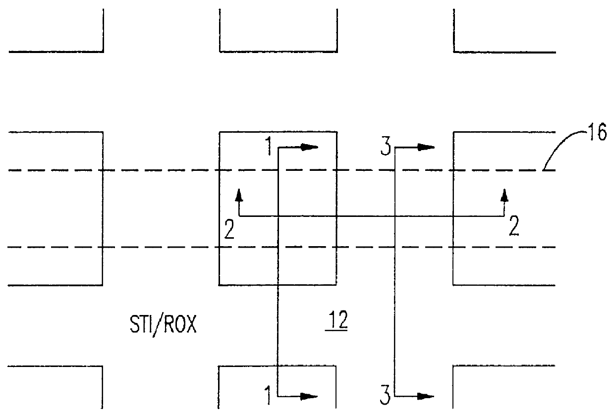
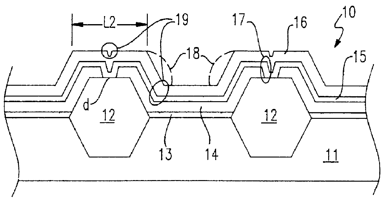
Referring now to the drawings, and more particularly to FIGS. 1 and 2, there is shown, in highly simplified cross-sectional form and plan view, respectively, an EEPROM or NVRAM gate structure 10 over which the present invention is an improvement. FIG. 2 is a plan view of the layout of the isolation structure 12 in the form of a grid and control gate 16 which is common to both the prior structure of FIG. 1 and the invention as will be described below. As to FIG. 2, however, the isolation structure is preferably a shallow trench isolation structure for practice of the invention rather than a recessed oxide structure shown in FIG. 1. However, a recessed oxide could also be employed in accordance with the principles of the invention.

In the structure 10 shown in FIG. 1, recessed oxide (ROX) 12 is used for isolation between adjacent gates. It is preferred that transistors including a floating gate for storage of charge be formed in very close proximity since the memory cells are programme...


PUM


Abstract

Recessing the floating gate of a NVRAM cell within a substrate or semiconductor layer between isolation structures permits manufacture by a simplified self-aligned process of high yield and economy while supporting maximum integration density and reducing or eliminating severe topography of the control gate connections which are formed in strips having a generally planar lower surface and which are of improved robustness and potentially fine pitch. Impurity implants are facilitated by thicknesses of various material present during portions of the process and in various combinations which may be advantageously exploited to obtain tailoring of impurity concentrations and profiles of both NVRAM cells and damascene field effect transistors formed by similar and compatible processes.

Description

1. Field of the InventionThe present invention generally relates to semiconductor integrated circuit memories field effect transistors and, more particularly, to non-volatile random access memory (NVRAM) structures and their manufacture.2. Description of the Prior ArtSemiconductor memory structures are well-known and designs thereof have been integrated at high densities, providing, at the present state of the art, several million dynamic memory cells or tens of thousands of static memory cells on a single chip along with decoding, addressing, sensing and driving circuits allowing data stored therein to be changed at will. Such memories and the speed of access they allow are indispensable to support the high speed of digital processors presently available. However, the maintenance of storage states of the cells requires at least constant application of at least stand-by power and, for dynamic memory cells, periodic refreshing. Since storage states are not otherwise maintained, such ...

Claims


Application Information

Patent Timeline
IPC IPC(8): H01L21/28H01L21/02H01L21/336
CPCH01L29/66825H01L21/28273H01L29/40114
Inventor BRACCHITTA, JOHN A.JOHNSON, JEFFREY B.MILES, GLEN L.
Owner IBM CORP
Learn More