Method and apparatus for electron-only radiation detectors from semiconductor materials

Inactive Publication Date: 2000-05-30
SANDIA
View PDF8 Cites 42 Cited by
  • Summary
  • Abstract
  • Description
  • Claims
  • Application Information

AI Technical Summary

Problems solved by technology

As previously stated, because of the deleterious effects of hole-tailing in semiconductor detectors, much effort has gone into attempting to solve this problem.
Neither of these approaches directly addresses the problem of eliminating hole-tailing.
This approach, however, also suffers from various drawbacks.
First, the grid structure is relatively complex and would be difficult, if not impossible, to use in detector arrays.
Second, the grids require two separate amplifying chains, plus a difference amplifier, adding significantly to the complexity and cost of manufacture.
This circuitry also would be difficult to implement in the multichannel type integrated circuits needed in detector array structures.
The primary disadvantage of McGregor

Method used


Image

  • Method and apparatus for electron-only radiation detectors from semiconductor materials
  • Method and apparatus for electron-only radiation detectors from semiconductor materials
  • Method and apparatus for electron-only radiation detectors from semiconductor materials

Examples


Embodiment Construction

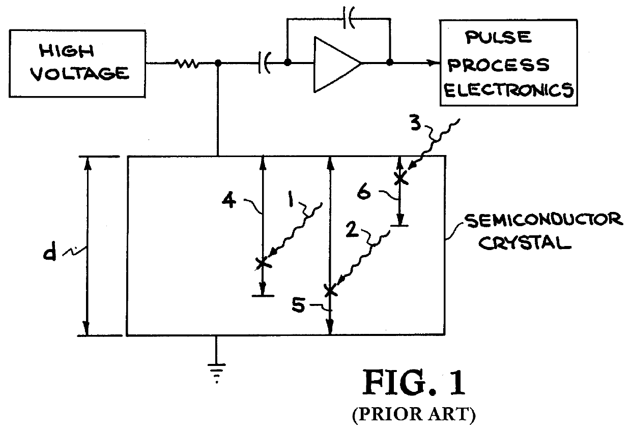
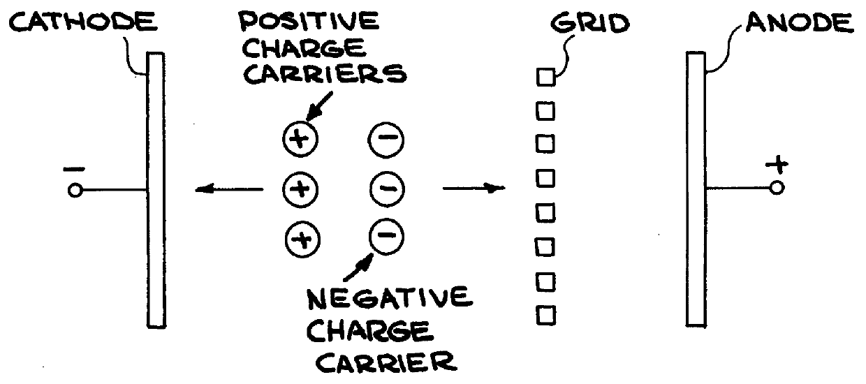
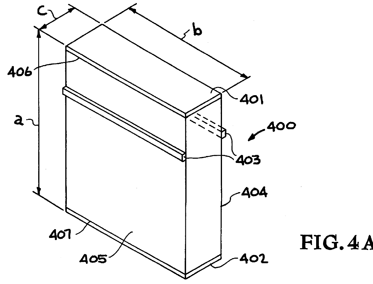
A new method for constructing an electron-only (unipolar) radiation detector has been conceived. FIG. 4A shows a perspective view of this new design in its simplest form. The detector crystal 400, consists of a piece of semiconducting material in the form of a rectangular parallelepiped with electrical contacts, or electrodes, placed on two opposing faces (anode 401 and cathode 402) as with any conventional detector. In addition to electrodes 401 and 402 on opposing faces, there are lateral contacts 403 placed on the lateral faces 404 and 405 (faces at right angles to anode and cathode contacts). Lateral contacts 403 serve to block charge induction from the motion of holes, serving much the same function as the grid in a Frisch Grid type gas detector. FIG. 4B illustrates the operation of the new device shown in FIG. 4A. Alternatively, there may be a single lateral contact spanning the perimeter of the crystal.

The reader will noted that FIG. 4A shows a perspective view of the preferr...


PUM


Abstract

A system for obtaining improved resolution in room temperature semiconductor radiation detectors such as CdZnTe and Hgl2, which exhibit significant hole-trapping. A electrical reference plane is established about the perimeter of a semiconductor crystal and disposed intermediately between two oppositely biased end electrodes. The intermediate reference plane comprises a narrow strip of wire in electrical contact with the surface of the crystal, biased at a potential between the end electrode potentials and serving as an auxiliary electrical reference for a chosen electrode-typically the collector electrode for the more mobile charge carrier. This arrangement eliminates the interfering effects of the less mobile carriers as these are gathered by their electrode collector.

Description

Semiconductors are materials which exhibit a band gap between the material's valence and conduction bands, typically no more than a few eV. Because this energy gap is so low, as the temperature of the crystal is increased, electrons are thermally excited and easily from the valance band to the conduction band. The electrical properties of these materials, therefore, are effected not only by the movement of electrons into the conduction band but also by the formation of vacant sites or "holes" in the valence bands left behind by the departing electrons. Both can conduct current.Holes also may be created by the interaction of energetic radiation, such as X-rays, gamma rays, and the like, with intrinsic semiconductors and, therefore, one should be able to use these materials as detectors for measuring high energy radiation. In fact, high-resistivity semiconductor radiation detectors are widely used for detecting ionizing radiation due to their ability to operate at room temperature, th...

Claims


Application Information

Patent Timeline
IPC IPC(8): H01L31/0264H01L31/0296H01L31/115
CPCH01L31/115H01L31/0296
Inventor LUND, JAMES C.
Owner SANDIA
Why Eureka
Try Eureka