
Method of fabricating semiconductor components

a technology of semiconductor components and components, applied in semiconductor/solid-state device testing/measurement, lapping machines, instruments, etc., can solve problems such as difficult implementation and inability to be reliabl

Inactive Publication Date: 2000-06-06
ALCATEL LUCENT SAS
View PDF10 Cites 5 Cited by
  • Summary
  • Abstract
  • Description
  • Claims
  • Application Information

AI Technical Summary

Benefits of technology

The present invention makes it possible to solve these problems. To this end, the method of the invention includes using at least one set of marker layers or "markers" that are separated by intermediate layers of different refractive index making it possible to produce a response signal (reflected signal) that includes a sequence representative of the index discontinuities between the markers and the intermediate layers.
According to another characteristic of the invention, the set of marker layers is constituted by an irregular alternation of marker layers and intermediate layers such that the refractive index discontinuities correspond to a sequence possessing an irregularity. This characteristic makes it possible to discriminate said sequence from a sequence corresponding to periodic noise or to distinguish said sequence from the sequence given by a structure having a periodic stack.
According to another characteristic of the invention, the method consists in causing a plurality of sets of marker layers separated by intermediate layers to be grown at distinct levels in the structure and producing sequences that are distinct due to the refractive index discontinuities of the layers constituting the sets. This characteristic makes it possible to monitor different depths of etching performed on the same structure.

Problems solved by technology

The method described above suffers from difficulties of implementation since it becomes uncertain when interfering peaks appear in the response signal or when the structure of the component presents multiple interfaces.
Unfortunately, that solution requires the rate of etching and the thickness of the material that is to be etched to be known so as to be able to open the detection and analysis window for the reflected signal when the depth of etching has come close to the position of the interface.
Furthermore, that method is not reliable since it does not make it possible to solve the problem of random peaks appearing.

Method used


Image

  • Method of fabricating semiconductor components
  • Method of fabricating semiconductor components
  • Method of fabricating semiconductor components

Examples


Embodiment Construction

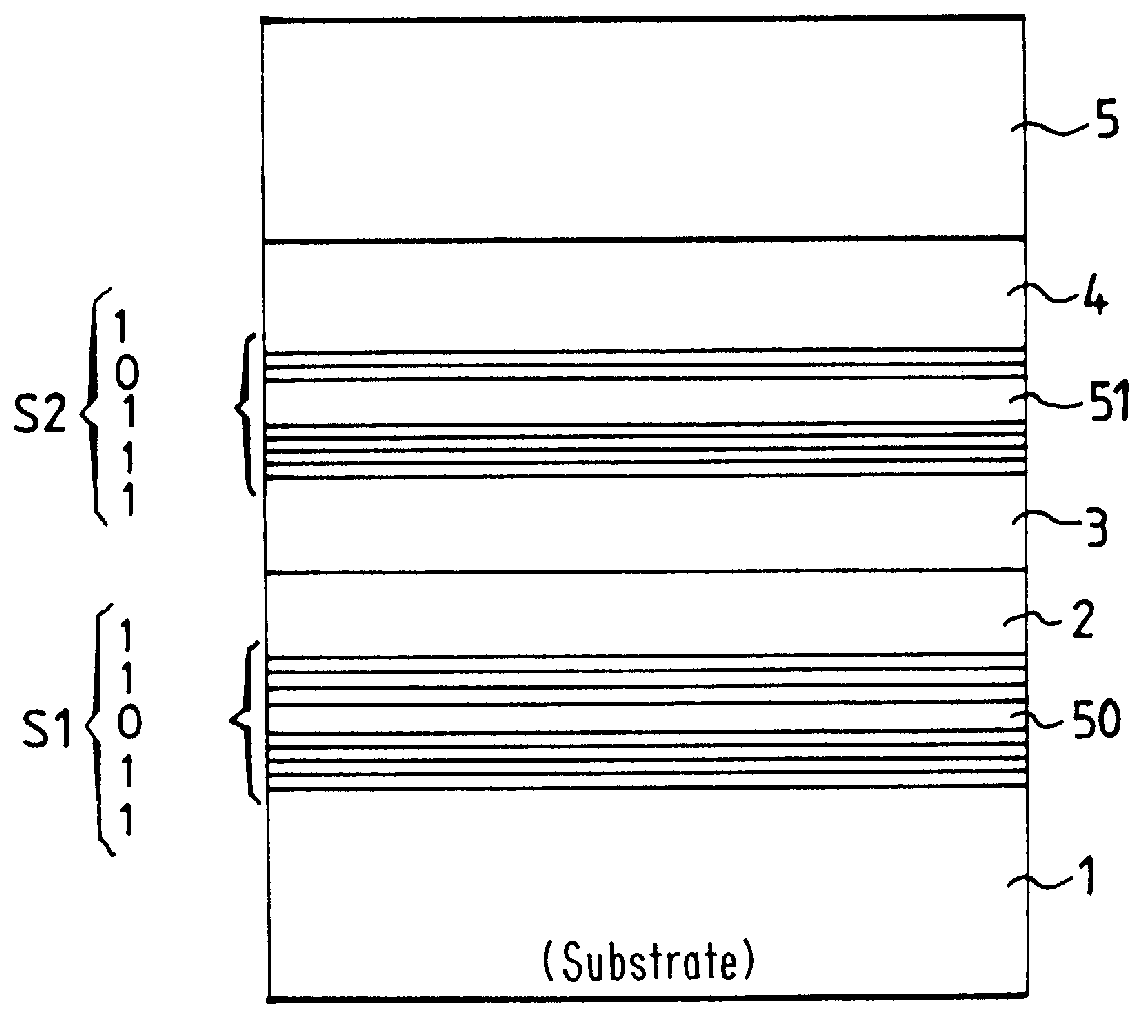
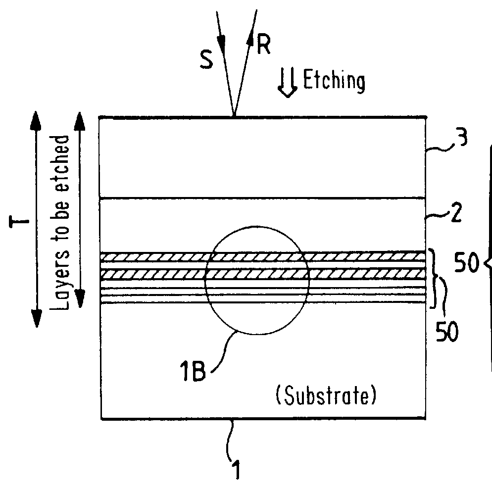
The description below relates to a simple semiconductor structure shown in the diagram of FIG. 1. This figure is a cross-section in the width direction through a structure that has not yet been etched.

Typically, and as shown in this example, the semiconductor structure comprises a substrate 1 made of indium phosphide (InP) doped with n-type carriers. The substrate may be covered in a buffer layer (not shown) for facilitating epitaxial growth of the various layers to be stacked, referred to below as the "upper" layers. The layers conventionally stacked on the substrate are constituted, for example, by a first layer-of quaternary material of the GaInAsP type buried under a layer made of a material of III-V type such as InP.

The invention applies to any other semiconductor structure, e.g. a structure using gallium arsenide, such as GaAs or AlGaAs.

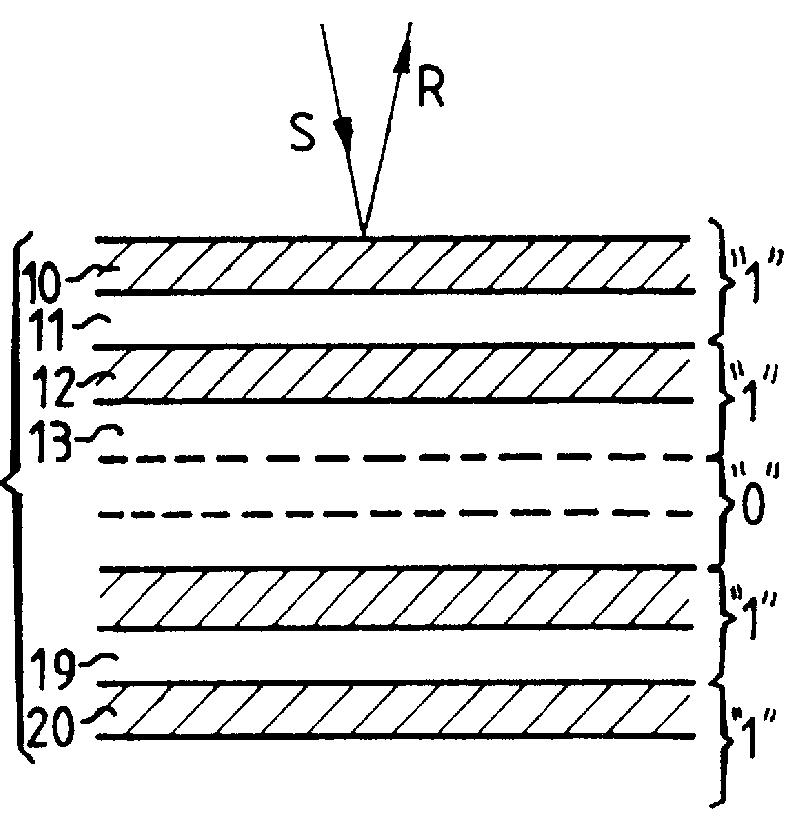
According to the method of the invention, epitaxy is used to grow on the substrate 1 a set 50 of marker layers 10, 12, . . . , 20 separated by...


PUM

PropertyMeasurementUnit
thicknessaaaaaaaaaa
thicknessaaaaaaaaaa
thicknessaaaaaaaaaa

Abstract

A method of fabricating a semiconductor component, the method including at least one step of etching an upper layer formed on a substrate. In the method, prior to forming the upper layer, at least one set made up of marker layers separated by intermediate layers of predetermined thicknesses is caused to be grown, where the marker layers and adjacent intermediate layers have different refractive indices, and then during etching of the upper layer refractive index discontinuities are detected optically and etching is stopped when the sequence of the optically detected discontinuities corresponds to a reference sequence representative of the thicknesses of the intermediate layers.

Description

The invention relates to a method of fabricating semiconductor components.The invention applies to monitoring the depth of etching while such components are being fabricated.Techniques for fabricating optoelectronic components make use of a dry etching technique such as reactive ion etching.Such techniques require in situ monitoring of the depth of etching into the structure constituting the component.It is common practice to use laser interferometry to perform such monitoring when the structure is made up of thin layers.Laser interferometry makes it possible to take measurements by means of a reflected laser beam while etching is taking place. The received response signal as reflected from the structure is a function-of the rate of etching and of the complexity of the refractive indices of said structure.During the etching of a structure made up of a various layers of material, each interface gives rise to a discontinuity in the reflected signal. The derivative of the signal (in th...

Claims


Application Information

Patent Timeline
Patent Type & Authority Patents(United States)
IPC IPC(8): G01B11/06H01L21/66H01L21/302C23F4/00H01L21/3065
CPCB24B37/013H01L22/26G01B11/0616
Inventor STARCK, CHRISTOPHELE GOUEZIGOU, LIONEL
Owner ALCATEL LUCENT SAS
Learn More