Method and apparatus for adapting an asynchronous bus to a synchronous circuit

a technology of asynchronous bus and synchronous circuit, which is applied in the direction of generating/distributing signals, duplex signal operation, instruments, etc., can solve the problems of not being able to employ all existing peripheral interface circuits on an asynchronous bus, not being able to support development tools, and being difficult to implement strict applications

Inactive Publication Date: 2000-06-13
NOKIA TECHNOLOGLES OY
View PDF11 Cites 33 Cited by
  • Summary
  • Abstract
  • Description
  • Claims
  • Application Information

AI Technical Summary

Problems solved by technology

An asynchronous bus may cause difficulties in applications that are strict as far as timing is concerned.
This results in certain drawbacks.
In addition, the fact that the transitions of the signals ENA' and RWN have not necessarily been synchronized to the system clock (CKO) may cause problems in applications that are critical as far as timing is concerned.
Furthermore, some ASIC circuit suppliers only have synchronous memories to offer, which means that it is not possible to employ all existing peripheral interface circuits on an asynchronous bus.
In addition, an environment requiring two control signals for timing is rather poorly, or not at all, supported by development tools.

Method used


Image

  • Method and apparatus for adapting an asynchronous bus to a synchronous circuit
  • Method and apparatus for adapting an asynchronous bus to a synchronous circuit
  • Method and apparatus for adapting an asynchronous bus to a synchronous circuit

Examples


Embodiment Construction

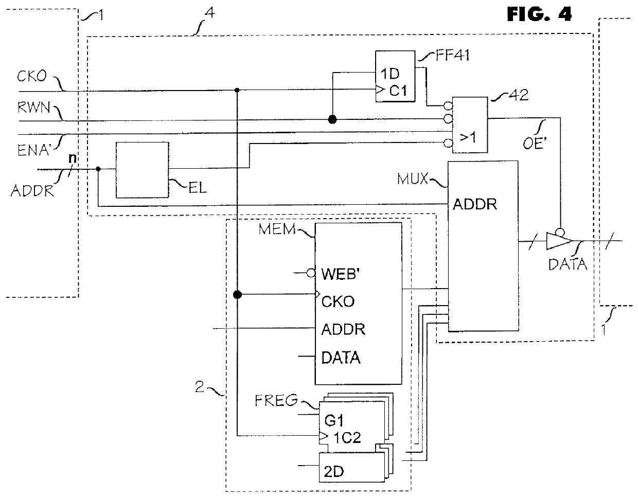
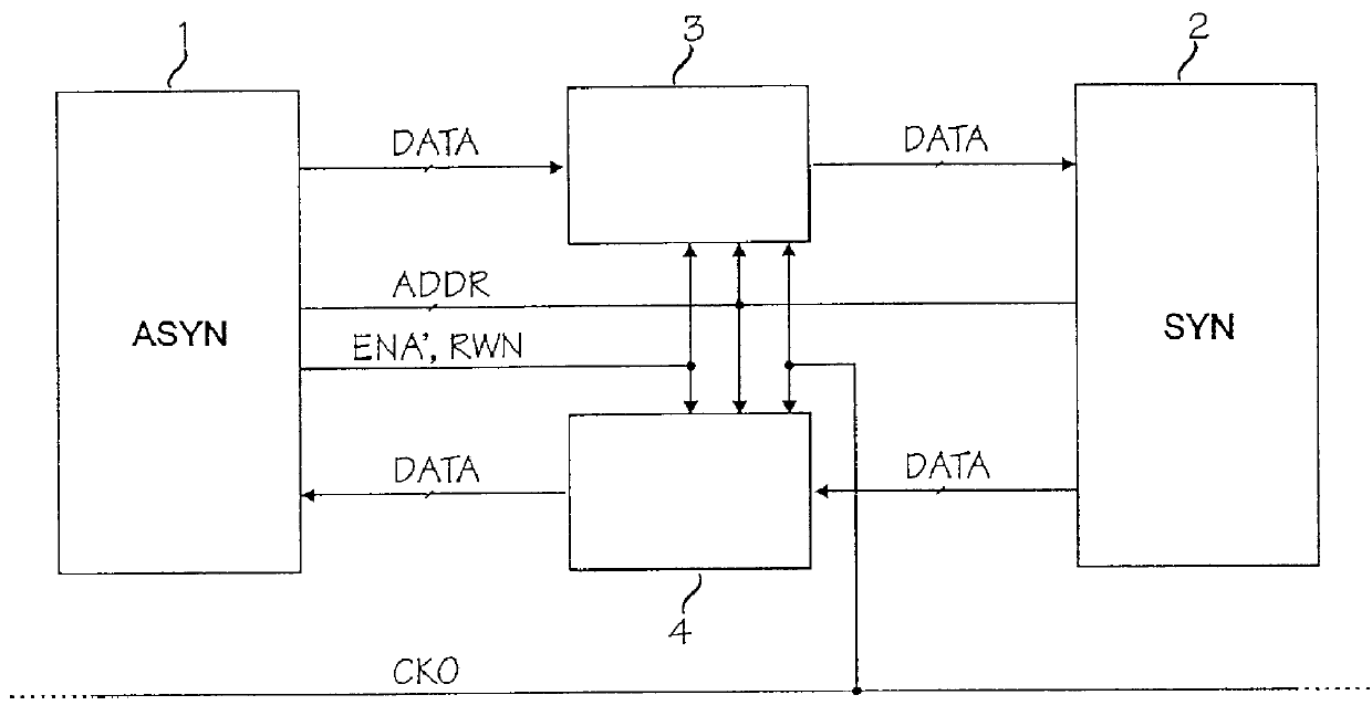
The positioning of the adapting interfaces of the invention are shown in FIG. 1. Between an asynchronous circuit 1 and a synchronous circuit 2 there is arranged an adapting interface 3, which carries out the transfer of data (DATA) from the asynchronous circuit 1 to the synchronous circuit 2, and an adapting interface 4 which carries out the transfer of data in the reverse direction. According to requirements at any one time, one or both adapting interfaces 3 and 4 of the invention can be used.

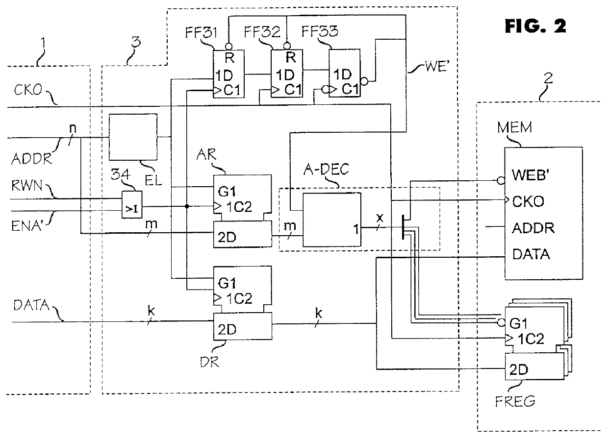
In the following, the operation of the adapting interface 3 of the invention is examined on the basis of FIG. 2 and the associated pulse diagram 3. The figures present the blocks that are essential to the invention: the asynchronous circuit 1 (e.g. a digital signal processor), the synchronous circuit 2 and the adapting interface 3 in accordance with the invention. In the pulse diagram 3, it is assumed that the write transaction employs a wait state WS and that there is one NOP (No Operation) i...


PUM


Abstract

PCT No. PCT/FI96/00285 Sec. 371 Date Nov. 28, 1997 Sec. 102(e) Date Nov. 28, 1997 PCT Filed May 23, 1996 PCT Pub. No. WO96/38793 PCT Pub. Date Dec. 5, 1996Many digital processors have an asynchronous bus controlled by two control signals. To interface a synchronous memory to an asynchronous bus, interface logic is required. In an interface for transferring data from an asynchronous circuit to a synchronous circuit, data to be written are written in an intermediate register while timing control signals are being synchronized to a system clock by means of flip-flops. Correspondingly, in an interface for transferring data from the synchronous circuit to the asynchronous circuit, a signal indicating a read transaction from the synchronous circuit is synchronized to the system clock by means of a flip-flop circuit.

Description

1. Field of the InventionThe present invention relates to an arrangement by which a circuit provided with an asynchronous bus can be adapted to peripheral interface circuits that require a synchronous bus.2. Description of the Related ArtMany digital processors have an asynchronous bus which is controlled by two timing control signals. An asynchronous bus may cause difficulties in applications that are strict as far as timing is concerned. The libraries of some producers of Application Specific Integrated Circuits (from hereafter "ASIC circuits") also contain synchronous memories only, or using such a memory instead of an asynchronous memory is otherwise feasible. In order to adapt a synchronous memory to an asynchronous bus, interface logic is required.In many digital processors, such as the AT&T.RTM. signal processor DSP1610, the bus is controlled by two timing control signals. In the figures, they are presented as signals ENA' and RWN. State 0 of the signal ENA' (Enable) indicate...

Claims


Application Information

Patent Timeline
Patent Type & Authority Patents(United States)
IPC IPC(8): G06F13/40G06F13/42
CPCG06F13/405
Inventor PIIRAINEN, OLLI
Owner NOKIA TECHNOLOGLES OY
Why Eureka
Try Eureka