Hold time margin increased semiconductor device and access time adjusting method for same

a technology of access time and access time, which is applied in the direction of digital storage, pulse automatic control, instruments, etc., can solve the problems of signal delay variation, signal delay variation, and dead band that cannot be compensated

Inactive Publication Date: 2000-06-27
SOCIONEXT INC
View PDF6 Cites 42 Cited by
  • Summary
  • Abstract
  • Description
  • Claims
  • Application Information

AI Technical Summary

Problems solved by technology

In addition, there are variations in signal delays on a circuit board mounting semiconductor devices.
Moreover, the signal delays vary depending on the variation of the temperature and the external voltage.
However, the present inventors have found that th

Method used


Image

  • Hold time margin increased semiconductor device and access time adjusting method for same
  • Hold time margin increased semiconductor device and access time adjusting method for same
  • Hold time margin increased semiconductor device and access time adjusting method for same

Examples


first embodiment

FIG. 1 shows a portion relating to an output circuit 23 of a semiconductor device 30. The output circuit 23 is structured, for example, as the third pipe 23A shown in FIG. 11. Data DAT is provided to the output circuit 23, held in synchronization with an internal clock jCLK provided to the control input thereof and outputted as data DQ to an external output terminal to which a load 31a is connected. The load 31a denotes the sum of a load at an input stage of the semiconductor device 31 shown in FIG. 12 and a load of a connecting line between semiconductor devices, and the value of the load 31a varies depending on the type of the interface.

An input circuit 24 has a electrostatic protection circuit and a buffer circuit for amplifying a signal driving performance, and amplifies the provided external clock CLK and outputs it as an internal clock iCLK. The clock iCLK is delayed by a variable delay circuit 32 and outputted therefrom as an internal clock jCLK.

The signal delay times in the ...

second embodiment

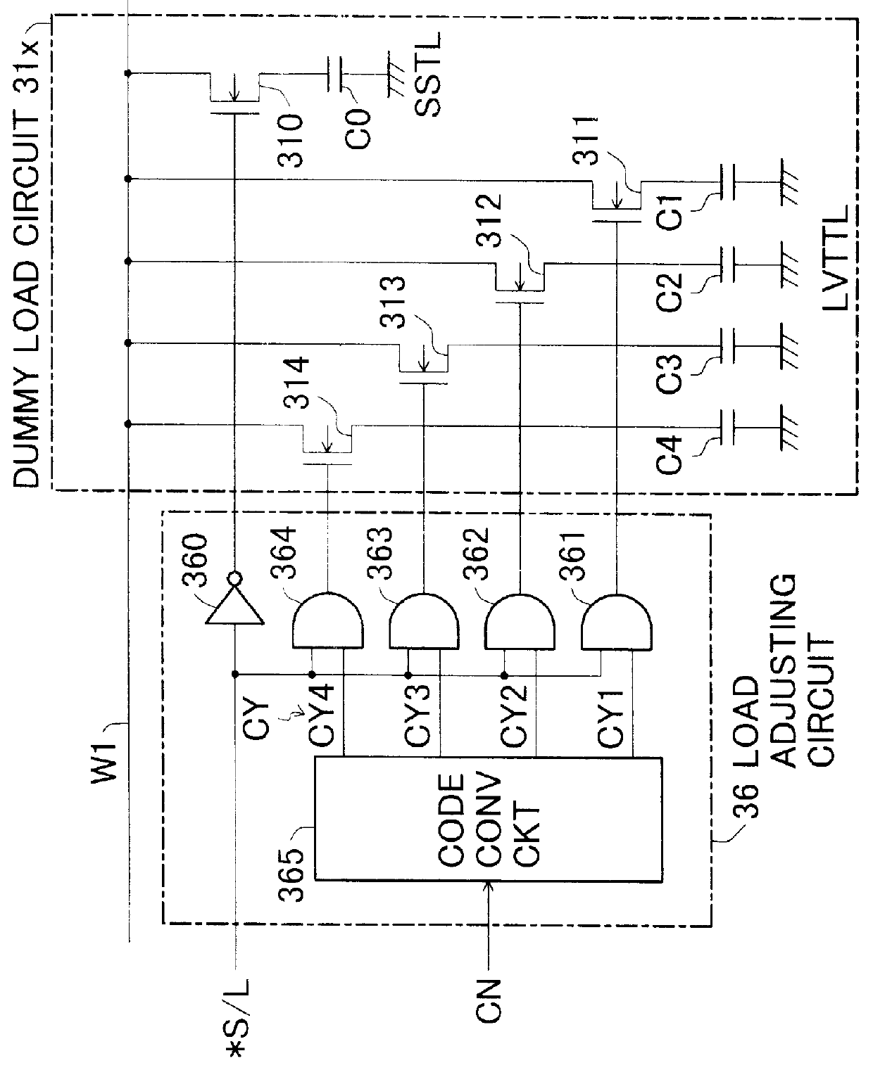
In the adjustment of item (C), the frequencies of the data DQ and the dummy data d.sub.-- DQ may be inverted every pulse of the external clock in a high frequency, namely at the maximum data frequency.

In this case, the value L2 of the load of the dummy load circuit 31x is determined as a value shifted by the value .DELTA.L from the proper value L1 of the load in the case that the access time ta does not depend on the frequency of the data DQ, where .DELTA.L corresponds to substantially a half of the maximum value of the deviation of the access time ta that varies corresponding to the frequency of the data DQ. Under this condition of L2=L1+.DELTA.L, the DDL circuit 40 is operated so as to adjust the delay time of the delay circuit 32. Namely, the delay adjusting circuit 39 controls the delay time of a delay circuit 32 so that the difference between the phases of the clock d.sub.-- iCLK and iCLK becomes a predetermined value.

Namely, with setting L2=L1+.DELTA.L, the DDL circuit 40 is o...


PUM


Abstract

A load adjusting circuit 36 adjusts the load value L=L2 of a dummy load circuit 31x corresponding to the outputs of a frequency determining circuit 37 and an interface determining circuit 35 as L2=L1- DELTA L holding, where L=L1 is a proper value in the case that the access time does not depend on the frequency of the data DQ and DELTA L corresponds to a half of the maximum value tlc of the deviation of the access time that varies corresponding to the frequency of the data DQ. A DLL circuit 40 delays a internal clock iCLK by a time delta tx so that a difference between phases of the clock iCLK and a dummy internal clock d-iCLK becomes a predetermined value. The delay time delta tx is equal to a value determined in such a way that delta tx=67 tx0 is determined with activating the DLL circuit 40, tlc is determined and delta tx is finally determined as delta tx= delta tx0+ tlc/2 or delta tx= delta tx0-tlc/2 due to the condition of data frequency at determining delta tx0.

Description

1. Field of the InventionThe present invention relates to a hold time margin increased semiconductor device and an access time adjusting method for the same.2. Description of the Related ArtFIG. 10 shows a schematic block diagram of part of a prior art synchronous DRAM. In the following description, a negative logic signal corresponding to a positive logic signal A will be designated as *A.With a row address decoded signal, a word line WL is activated to select a line in a cell array 10. Data read from the line is amplified by a sense amplifier 11. For instance, according to data read from a memory cell 12, a weak voltage takes place between a pair of bit lines BL and *BL and this voltage is amplified by the sense amplifier 11. Next, with a column address decoded signal, a column selecting line CL is activated to selectively turn on a switch in a column switch circuit 13, thereby a pair of bit lines BL and *BL are connected to a pair of data bus lines DB and *DB, respectively. Volta...

Claims


Application Information

Patent Timeline
IPC IPC(8): G11C7/10G11C7/00G11C7/22H03L7/081H03L7/08H03L7/089G11C11/407G11C11/409H01L21/822H01L27/04H03L7/06
CPCG11C7/1051H03L7/0814G11C7/22H03L7/089H03L7/0816G11C11/34
Inventor DOUCHI, HIROKOSHINOZAKI, NAOHARU
Owner SOCIONEXT INC
Why Eureka
Try Eureka