Test structure for monitoring overetching of silicide during contact opening

a test structure and silicide technology, applied in semiconductor/solid-state device testing/measurement, semiconductor device details, semiconductor/solid-state device testing/measurement, etc., can solve the problem of easy error in substituting the actual wafer with a blank one, insufficient sem method, and difficult wafer mapping

Inactive Publication Date: 2000-07-11
NAT SCI COUNCIL
View PDF3 Cites 47 Cited by
  • Summary
  • Abstract
  • Description
  • Claims
  • Application Information

AI Technical Summary

Problems solved by technology

However, SEM method is not precise enough, destructive and time consuming, making wafer-mapping rather difficult.
Furthermore, the blank test wafer method

Method used


Image

  • Test structure for monitoring overetching of silicide during contact opening
  • Test structure for monitoring overetching of silicide during contact opening
  • Test structure for monitoring overetching of silicide during contact opening

Examples


Embodiment Construction

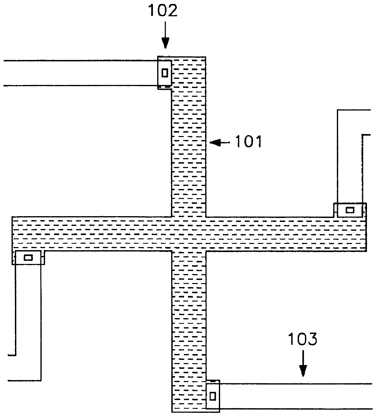
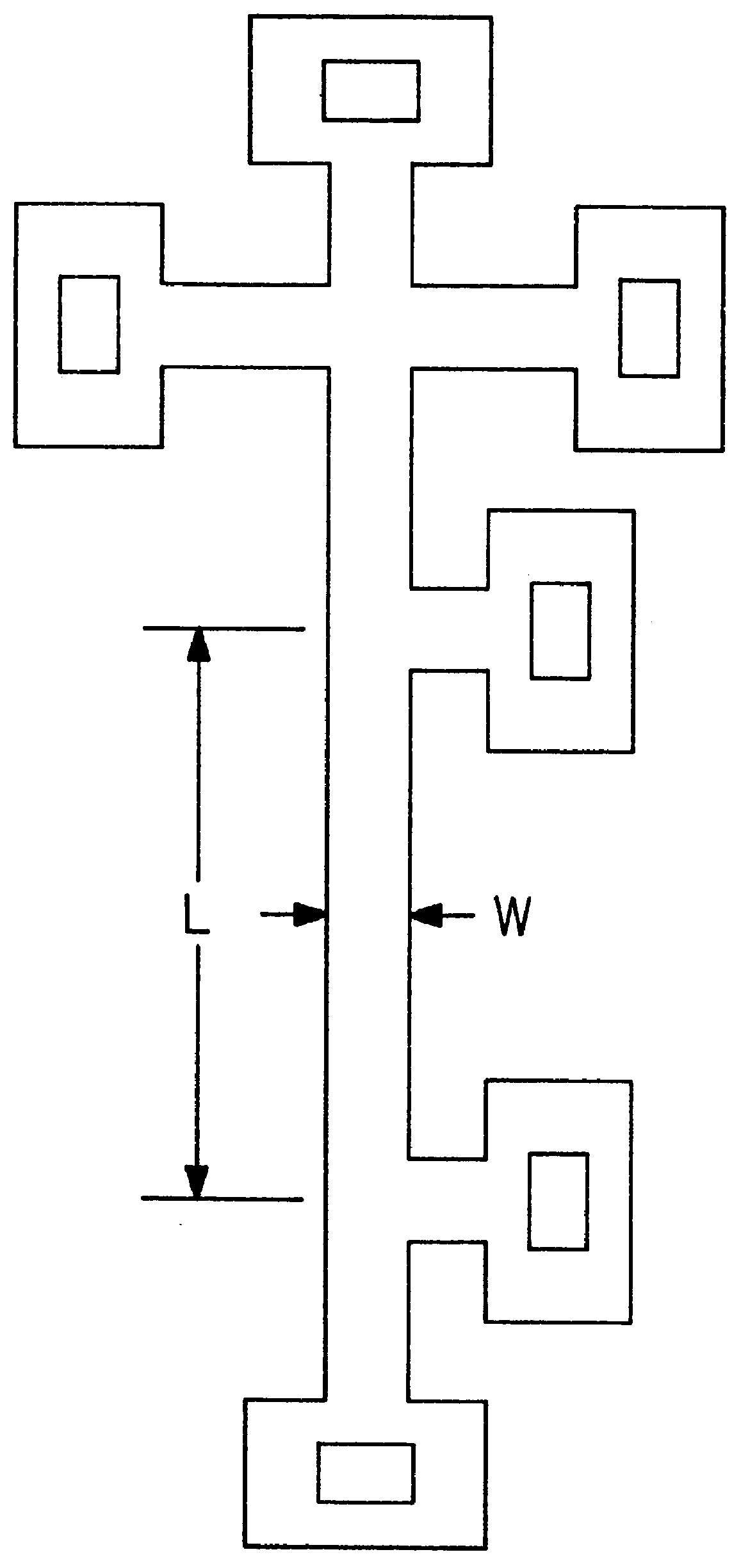
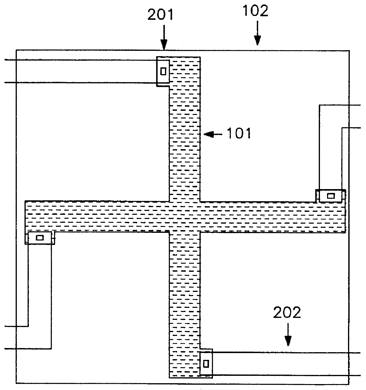
The principle of "the Electrical Detecting Method in Monitoring the Intactness of the Silicide layer on Source / Drain / Gate during Contact Layer Opening" of this invention is simple and practical. It is derived from the conventional van der Pauw test structure as shown in FIG, 1a or the cross-bridge structure as shown in FIG, 1b. Based on 1978 J. Electrochemical Society, 125 Issue, pp.645-650 and pp. 650-654 as shown in FIG, 1a documented by M. G. Buehler and etc, van der Pauw test structure can be applied to measure the sheet resistance of the conductor layer in deriving its thickness. The relevant contents lie in the four(4) contact holes at the 4 ends of the van der Pauw test structure which can be used for connecting with external wires. These four wires can be separately connected to voltage meter and current meter in deriving the sheet resistance of the van der Pauw centre. In addition, the cross-bridge structure, as the name suggests, contains a van der Pauw and a bridge. The e...


PUM


Abstract

For the contact opening in advanced IC processing, it becomes critical to monitor the degree of overetching of the thin silicide layer and also to obtain the etching rate of the silicide layer. A method is disclosed which will allow the electrical measurements of the sheet resistance of the exposed (by the contact etch) silicide layer, thus allowing electrical measurements to the integrity as well as the thickness of the remaining silicide layer. A main feature of the disclosed test method is a modification of the conventional van der Pauw test structure, or of the cross-bridge structure (which will allow electrical measurement of the line width, in addition to the sheet resistance information). Contrary to the conventional van der Pauw structure or cross-bridge structure where the contact opening pattern is designed to expose only the specific areas needed for allowing electrical connection to the four measurement pads, the contact opening mask is designed to expose some or all of the van der Pauw or cross-bridge structure, thus allowing the electrical measurement of the degree of silicide overetching during contact opening. The disclosed test method and corresponding structure can be applied as an on-wafer process monitor tool following the complete normal process flow, thus serving as a convenient on-wafer monitor.

Description

TECHNIQUE SCOPETo prevent the degradation of the transistor's electrical performance caused by parasitic resistors in the source / drain sector, silicidation of source / drain is commonly applied during the production of down-sizing micro-chip. Generally, such technology can be achieved by the silicidation of source / drain or self-aligned silicidation. However, along with further down-sizing of chips, the junction of source / drain also becomes shallower; the thickness of silicidated layer on source / drain must be thin down accordingly to prevent leaky junction. For instance, the technology applied in 0.18 .mu.m design rule requires junction thickness of less than 0.1 .mu.m; the thickness of the source / drain silicide layer is probably only 0.01-0.04 .mu.m. Such thin layer can be easily overetched during the contact opening while maintaining the uniformity and production, resulting in loss of function.Consequently, effective measuring and monitoring of the etching progress on this source / dra...

Claims


Application Information

Patent Timeline
IPC IPC(8): H01L23/544
CPCH01L22/34H01L2924/0002H01L2924/00
Inventor HUANG, TIAO-YUAN
Owner NAT SCI COUNCIL
Why Eureka
Try Eureka