Semiconductor device and manufacturing method

a technology of semiconductor devices and manufacturing methods, applied in semiconductor devices, semiconductor/solid-state device details, electrical apparatus, etc., can solve the problem that the method has not yet been widely adopted in conventional equipment for domestic us

Inactive Publication Date: 2000-07-11
TEXAS INSTR INC
View PDF2 Cites 84 Cited by
  • Summary
  • Abstract
  • Description
  • Claims
  • Application Information

AI Technical Summary

Problems solved by technology

However, due to problems with respect to reliability and handling in assembly, this method has not yet been widely adopted in conventional equipment for domestic use.

Method used


Image

  • Semiconductor device and manufacturing method
  • Semiconductor device and manufacturing method
  • Semiconductor device and manufacturing method

Examples


Embodiment Construction

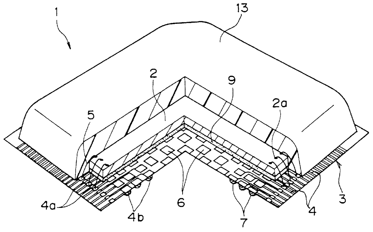
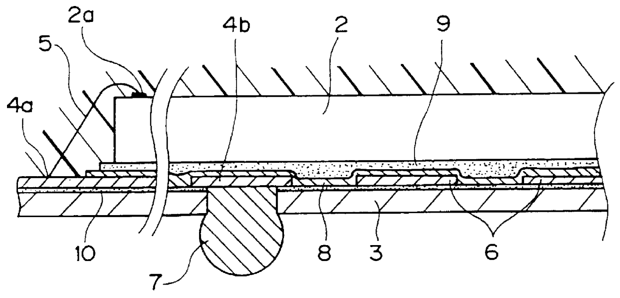
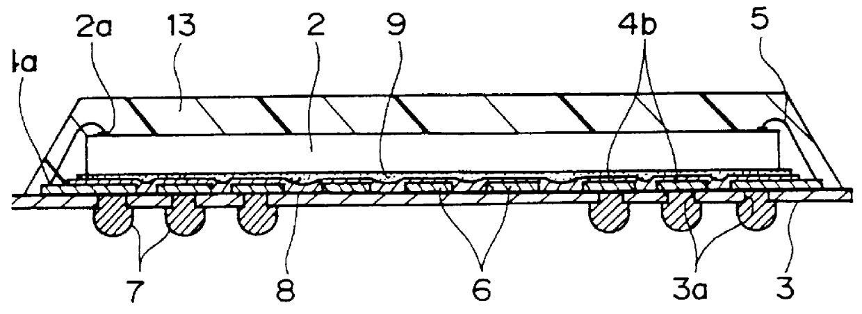
In the following, an embodiment of the present invention will be explained with reference to the figures. FIGS. 1 and 2 illustrate the semiconductor device as a CSP type package of the present invention. Semiconductor device (1) has insulating substrate (3) which has a plane size larger than that of IC chip (2). As an application example, insulating substrate (3) is made of a square shaped polyimide film with sides 12 mm long and 0.075 mm thick.

On the surface of insulating substrate (3), plural copper pattern elements (4) are formed to form electrical connections between IC chip (2) and solder bumps (7) as the external connecting terminals. For each copper pattern element (4), one end is positioned on through-hole (3a) formed on insulating substrate (3) and is connected through said through-hole (3a) to solder bump (7). In the present specification, this region will be called bump connecting land (4b) hereinafter. Bump connecting lands (4b) of the various copper pattern elements are...


PUM


Abstract

To completely suppress or minimize the voids formed between the insulating substrate and the IC chip in order to prevent the problems of separation and cracking of the chip caused by the aforementioned voids. The present invention is preferably adopted for the Chip Six Package type package or other package types equipped with solder bumps or other external connecting terminals directly beneath the IC chip. For insulating substrate (3), on its chip-carrying surface, there is pattern element (6) in the region beneath the IC chip and free of conductor pattern elements (4) in addition to conductor pattern element (4) for forming electrical connection between the electrode pads and the external connecting terminals of the chip. Said pattern element (6) divides said region into plural small regions A. IC chip (2) is bonded through die paste on insulating substrate (3) such that an end of conductor pattern element (4), pattern element (6) and divided small regions A are covered. Pattern element (6) acts to reduce the shifting of die paste (9) before curing due to the surface tension. As a result, the formation of voids beneath the chip can be completely prevented or minimized.

Description

The present invention pertains to a type of package structure of semiconductor device and its manufacturing method. In particular, the present invention pertains to a CSP type IC package.PRIOR ARTIn order to meet the demand for smaller size and higher speed in electronic information equipment, efforts have been made to develop technologies to reduce the size of the semiconductor devices carried in them. From the viewpoint of high-density assembly, the so-called bare assembly, in which the conventional package form that provides physical and chemical protection to the IC chip by means of package or the like is omitted, is believed to be the ultimate assembly method. However, due to problems with respect to reliability and handling in assembly, this method has not yet been widely adopted in conventional equipment for domestic use. CSP (Chip Size Package) refers to a high-density package with the size of the IC package equal to or slightly larger than the chip. Like the conventional pa...

Claims


Application Information

Patent Timeline
Patent Type & Authority Patents(United States)
IPC IPC(8): H01L21/58H01L21/02H01L23/28H01L23/31H01L23/12
CPCH01L23/3121H01L24/27H01L24/32H01L24/743H01L24/83H01L24/29H01L2224/32057H01L2224/32225H01L2224/48091H01L2224/48227H01L2224/48465H01L2224/73265H01L2224/743H01L2224/83192H01L2224/83385H01L2224/8385H01L2224/92H01L2224/92247H01L2924/01004H01L2924/01005H01L2924/01015H01L2924/01029H01L2924/01079H01L2924/01082H01L2924/07802H01L2924/14H01L2924/15311H01L2924/00014H01L24/48H01L2224/2919H01L2924/01006H01L2924/01023H01L2924/01033H01L2924/01045H01L2924/014H01L2924/0665H01L2924/00H01L2924/3512H01L24/49H01L2224/49175H01L2924/15183H01L2924/181H01L2924/00012H01L2224/45099H01L2224/05599H01L2224/85399H01L2224/45015H01L2924/207
Inventor ANO, KAZUAKIMURATA, KENSHO
Owner TEXAS INSTR INC
Why Eureka
Try Eureka