Voltage judgment circuit and battery cell pack having the same
- Summary
- Abstract
- Description
- Claims
- Application Information
AI Technical Summary
Benefits of technology
Problems solved by technology
Method used
Image
Examples
embodiment 1
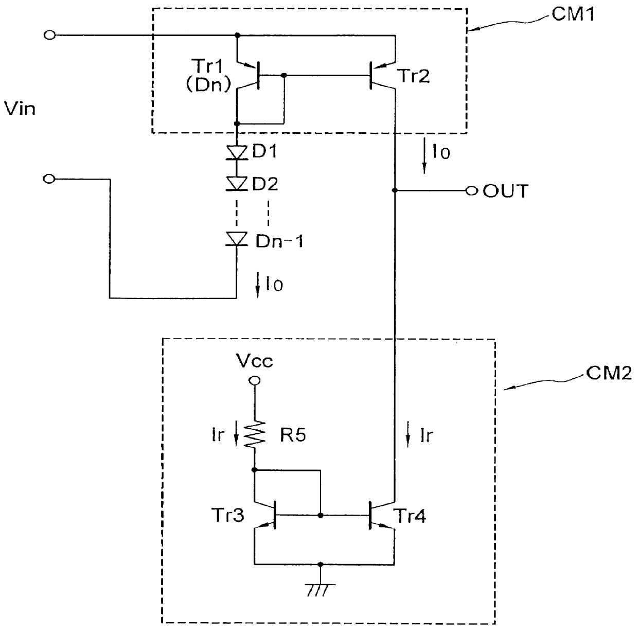
FIG. 2 is a circuit diagram showing a voltage judgment circuit of the present invention in accordance with a first Embodiment. A voltage judgment circuit of the present Embodiment has "n-1" diodes D1 to Dn-1 connected in series inserted in the forward direction of a judgment voltage, a first current mirror circuit CM1 for extracting a forward direction current of the diodes and a second current mirror circuit CM2 for obtaining and extracting a reference current.
Each of the diodes D1 to Dn-1 is formed by a diode-connected PNP transistor having a base and a collector connected with each other. The first current mirror circuit CM1 has a diode-connected first PNP transistor Tr1 of a reference side having a current path connected in series with the diodes D1 to Dn-1, and a second PNP transistor Tr2 of an output side having a base connected to the commonly connected base and collector of the first PNP transistor. Each of the "n-1" diodes D1 to Dn-1 have the same structure. The current cha...
embodiment 2
FIG. 4 is a circuit diagram showing a voltage judgment circuit of a second Embodiment. The voltage judgment circuit of the present Embodiment is different from that of the first Embodiment in that NPN transistors are employed as the diodes D1 to Dn and as the first current mirror circuit CM1, a third current mirror circuit CM3 is formed between the first current mirror circuit CM1 and the second current mirror circuit CM2, and an output terminal (OUT) is formed at a connection node between an output side transistor Tr8 of the third current mirror circuit CM3 and the output side transistor Tr4 of the second current mirror circuit CM3.
Since, in case of employing a plurality of the voltage judgement circuits, the respective "H" levels of the outputs of each of the voltage judgment circuits can be made to be the same high potential Vcc by constituting the diodes D1 to Dn by the NPN transistors in the voltage judgment circuit of the present Embodiment, the constitution of a next stage ci...
PUM
 Abstract
Description
Claims
Application Information


