Polysilicon defined diffused resistor

a technology of diffused resistor and polysilicon, which is applied in the direction of resistor details, resistors, electrical equipment, etc., can solve the problems of limiting the use of polysilicon in very high speed applications, requiring large silicon area in practical implementation, and low sheet resistivity of polysilicon

Inactive Publication Date: 2000-08-15
PMC-SIERRA
View PDF14 Cites 27 Cited by
  • Summary
  • Abstract
  • Description
  • Claims
  • Application Information

AI Technical Summary

Problems solved by technology

However, in a single-polysilicon complementary metal oxide silicon (CMOS) process the polysilicon has a very low sheet resistivity.
As a result it requires large silicon area in practical implementations.
In addition it has large parasitic capacitance (of the gate oxide) to silicon substrate, limiting its usage in very high

Method used


Image

  • Polysilicon defined diffused resistor
  • Polysilicon defined diffused resistor
  • Polysilicon defined diffused resistor

Examples


Embodiment Construction

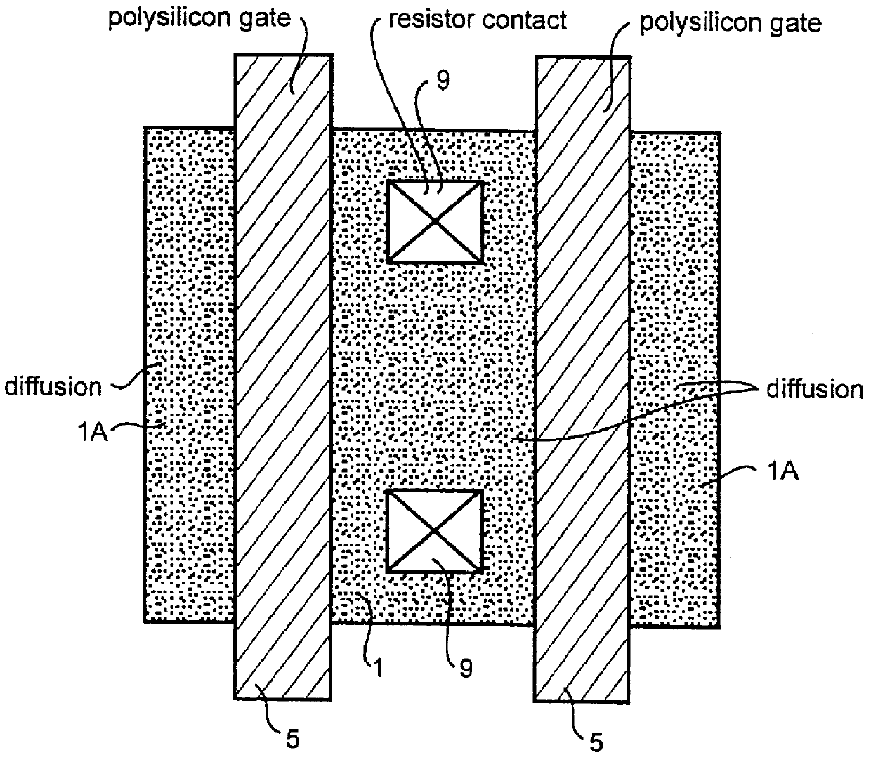
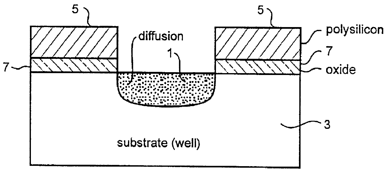
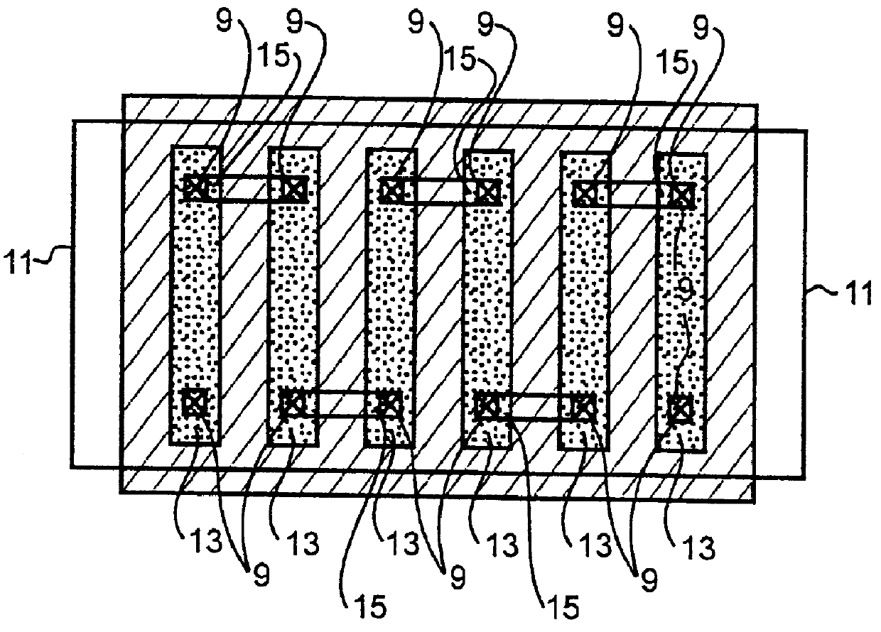
Turning to FIGS. 1 and 2, a central diffused region 1 is formed in a well known manner by diffusion of an impurity of a particular conductivity type into a well 3 of opposite conductivity type contained within or supported on a substrate (not shown). The impurity can be either n-type or p-type; however in a typical n-well integrated circuit process, p-type diffusion is preferable since the resistor is placed in an n-well region, thus being effectively isolated from the remainder of the integrated circuitry.

The diffused region is bounced on its sides by a polysilicon conductive layer 5 completely insulated by an insulating layer 7. That is, the conductive layer extends over the upper surface boundary and predetermined parts of the diffused region and the well.

In the case of the integrated circuit being silicon, the conductive layer 5 is preferably formed of polysilicon, and the insulating layer is preferably formed of silicon dioxide. The conductive layer 5 comprises a gate.

The condu...


PUM


Abstract

A resistor having a diffused impurity region in a semiconductor substrate, an insulated gate surrounding and defining the resistor, and a pair of separated conductive contacts to the diffused region within the boundary of the insulated gate for applying and receiving current passing through the resistor.

Description

This invention relates to the field of integrated circuits, and in particular to a resistor for an integrated circuit.BACKGROUND TO THE INVENTIONResistors are commonly used in integrated circuits such as silicon integrated circuits. For application in analog or in mixed mode analog and digital circuits, matching properties of resistors are very important.Two types of resistors are generally used in integrated circuits: polysilicon resistors, and diffused resistors. In a conventional single-polysilicon CMOS process, to obtain good matching properties both types of resistors occupy large silicon area, for the following reasons.The polysilicon resistor has good matching properties for the reason that its width is determined by a width of the silicon gate, which is a very tightly controlled dimension in a semiconductor manufacturing process. However, in a single-polysilicon complementary metal oxide silicon (CMOS) process the polysilicon has a very low sheet resistivity. As a result it ...

Claims


Application Information

Patent Timeline
IPC IPC(8): H01L29/66H01L29/8605H01L27/08H01L27/06H01L21/822H01L27/04
CPCH01L27/0629H01L27/0802H01L29/8605
Inventor INIEWSKI, KRISGERSON, BRIAN D.HARRIS, COLINLEBLANC, DAVID
Owner PMC-SIERRA
Why Eureka
Try Eureka