LCD and fabrication method thereof having a pedestal and overlying organic film at a periphery of the display

a technology of liquid crystal display and organic film, which is applied in the direction of instruments, non-linear optics, optics, etc., can solve the problems of inability to remove photoresist, increase the thickness of light shielding layer, and deteriorate the aperture ratio of each pixel

Inactive Publication Date: 2000-08-15
KK TOSHIBA
View PDF5 Cites 40 Cited by
  • Summary
  • Abstract
  • Description
  • Claims
  • Application Information

AI Technical Summary

Problems solved by technology

Thus, the aperture ratio of each pixel deteriorates.
However, when the thickness of the light shielding layer is increased, the following problem occurs.
When the pattern is developed, the photoresist cannot be satisfactorily removed.
In particular, when the conductive film remains in the stage portion on the periphery of the light shielding layer, lines in the vicinity of the light shielding layer short-circuit.
Thus, display defects, and consequently, product defects, occur.

Method used


Image

  • LCD and fabrication method thereof having a pedestal and overlying organic film at a periphery of the display
  • LCD and fabrication method thereof having a pedestal and overlying organic film at a periphery of the display
  • LCD and fabrication method thereof having a pedestal and overlying organic film at a periphery of the display

Examples


first embodiment

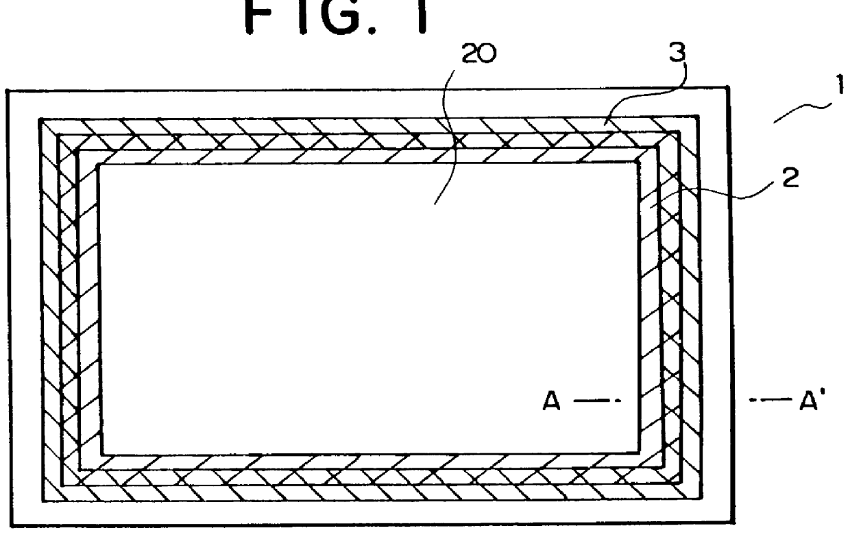
FIG. 1 is a plan view showing a switching device array substrate 1 in a liquid crystal displaying apparatus viewed from an opposite substrate 1'. In FIG. 1, for simplicity, a display area 20 in a cell is omitted. As is known, a plurality of switching devices are disposed in a matrix shape on a glass substrate of a switching device array substrate 1 of the liquid crystal displaying apparatus. Each of the switching devices has a drain electrode, a source electrode, and a gate electrode. The drain electrode is connected to a signal line. The source electrode is connected to a pixel electrode. The gate electrode is connected to a scanning line. A plurality of lines 10 of these signal lines and scanning lines extend to the outside of the display area 20 through a seal portion surrounded by the seal member 3. The lines 10 are connected to a signal line driving circuit, a scanning line driving circuit, and so forth disposed outside the substrate 1 or in the vicinity thereof.
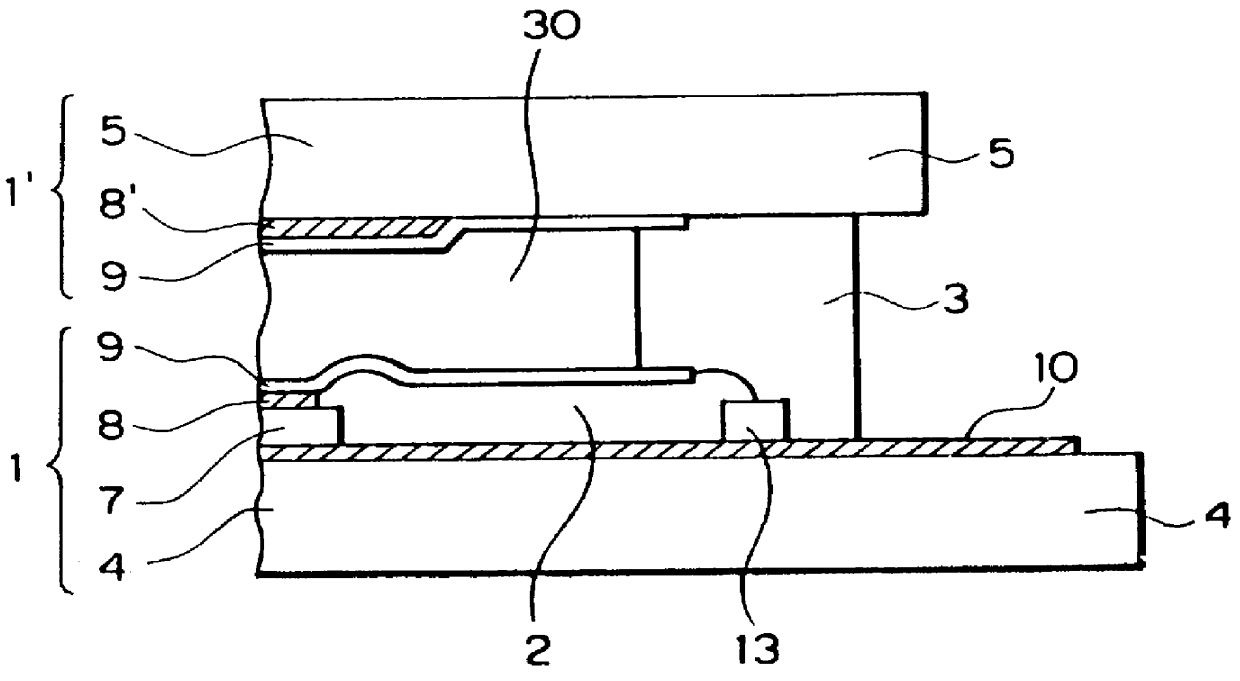
FIG. 2 is a sec...

second embodiment

Next, a liquid crystal displaying apparatus according to a second embodiment of the present invention will be described.

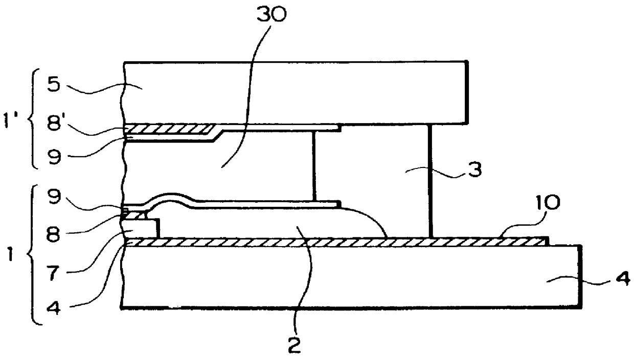
FIG. 4 is a sectional view showing the structure of the liquid crystal displaying apparatus according to the second embodiment of the present invention.

As shown in FIG. 4, according to the second embodiment, a pedestal is not formed on a seal portion. An edge portion of an organic film 2 is tapered in the direction of the outer peripheral portion of the substrate. Other structures thereof are the same as those of first embodiment.

Experimental results of the liquid crystal displaying apparatus fabricated in the above-described method show that the pixel electrode film does not almost remain on the periphery of the organic film 2 and short-circuit of lines due to the pixel electrode film that remained remarkably decreases. Consequently, the operational defect of the apparatus was almost prevented. Thus, liquid crystal displaying apparatus could be obtained with a hig...


PUM

PropertyMeasurementUnit
thicknessaaaaaaaaaa
areaaaaaaaaaaa
shapeaaaaaaaaaa

Abstract

A liquid crystal displaying apparatus is disclosed, that comprises a pair of substrates, a liquid crystal material filled in the space between the pair of substrates, a plurality of lines formed on one of the pair of substrates, an organic film formed on the plurality of lines, a conductive film formed on the organic film, and a pedestal, wherein the plurality of lines extend from a first area to a second area, the organic film being disposed on the plurality of lines in the first area, the second area exceeding an edge portion of the organic film, wherein the pedestal is disposed between the first area and the second area through the edge portion, wherein the organic film is formed between the pedestal to a non-pedestal area, wherein the thickness in the vicinity of at least the edge portion of the organic film formed on the pedestal is smaller than the thickness of the organic film formed in the non-pedestal area, and wherein the thickness of the pedestal is smaller than the thickness of the organic film formed in the non-pedestal area.

Description

1. Field of the InventionThe present invention relates to a liquid crystal displaying apparatus and a fabrication method thereof.2. Description of the Related ArtIn recent years, to accomplish a high speed picture process and a high quality display picture of a liquid crystal displaying apparatus, an active matrix drive type color liquid crystal displaying apparatus has been widely used. In this color liquid crystal displaying apparatus, switching thin film transistors are disposed for individual display pixels.Generally, in a liquid crystal displaying apparatus, two glass substrates having electrodes are sealed with an adhesive agent and a sealing agent. Liquid crystal material is filled in the space between the two glass substrates. To keep the distance between the two substrates constant, plastic beads, or the like, with equal particle diameters are dispersed as spacers between the substrates. In a color liquid crystal displaying apparatus, a color filter layer having a color lay...

Claims


Application Information

Patent Timeline
Patent Type & Authority Patents(United States)
IPC IPC(8): G02F1/1333G02F1/13G02F1/1335G02F1/1339
CPCG02F1/133512G02F1/1339G02F2001/133388G02F1/133388G02F1/136209G02F1/134309
Inventor KUROSAKI, MINAKOMIDORIKAWA, TERUYUKI
Owner KK TOSHIBA
Why Eureka
Try Eureka