
System management interrupt for a desktop management interface/system management basic input output system interface function

Inactive Publication Date: 2000-09-19
HEWLETT PACKARD DEV CO LP
View PDF7 Cites 48 Cited by
  • Summary
  • Abstract
  • Description
  • Claims
  • Application Information

AI Technical Summary

Benefits of technology

In accordance with the present invention, during a manufacturing process for the computing system, BIOS may access a protected memory space by triggering a system management interrupt (SMI). The SMI causes the OS to enter a system management mode (SMM). In SMM, the processor is capable of accessing the entire memory address space without risking a memory protection fault. In addition, the entry into SMM enables BIOS to make use of system management memory (SMRAM) that is reserved for the SMM, alleviating the problem of limited work buffer area. A SMI handler routine calls a DMI / SMBIOS function, such as function 52h (Set Structure), to update an original equipment manufacturer (DEM) string or other database information.

Problems solved by technology

A major disadvantage of ROM BIOS is that it must be loaded into the ROM device when the computer system is manufactured, making the ROM BIOS difficult to update when new types of devices are added to the computer system.
One limitation of flash ROM is that the contents must be altered in blocks instead of individual bytes as is common with other memory devices such as RAM and hard disk drives.
However, when the Basic Input Output System (BIOS) needs to update the MIF database directly a couple of problems have typically arisen.
Typically, the work area recommended by DMI / SMBIOS specifications has not been sufficient.
Although non-volatile memory can be located anywhere in memory space, an attempt by BIOS to access memory space has at times caused a memory protection fault by violating memory access rights set by an operating system (OS).

Method used


Image

  • System management interrupt for a desktop management interface/system management basic input output system interface function
  • System management interrupt for a desktop management interface/system management basic input output system interface function
  • System management interrupt for a desktop management interface/system management basic input output system interface function

Examples


Embodiment Construction

This application is related to the following copending and commonly assigned United States patent applications which are hereby incorporated by reference as if set forth in their entirety:

U.S. patent application Ser. No. 09 / 070,866, entitled "A METHOD FOR FLASHING ESCD AND VARIABLES INTO A ROM" to Mark A. Piwonka, Louis B. Hobson, Jeffrey D. Kane, and Randall L. Hess; and

U.S. patent application Ser. No. 09 / 070,823, entitled "METHOD OF FLASH PROGRAMMING OR READING A ROM OF A COMPUTER SYSTEM INDEPENDENTLY OF ITS OPERATING SYSTEM" to Patrick L. Gibbons and Paul J. Broyles III.

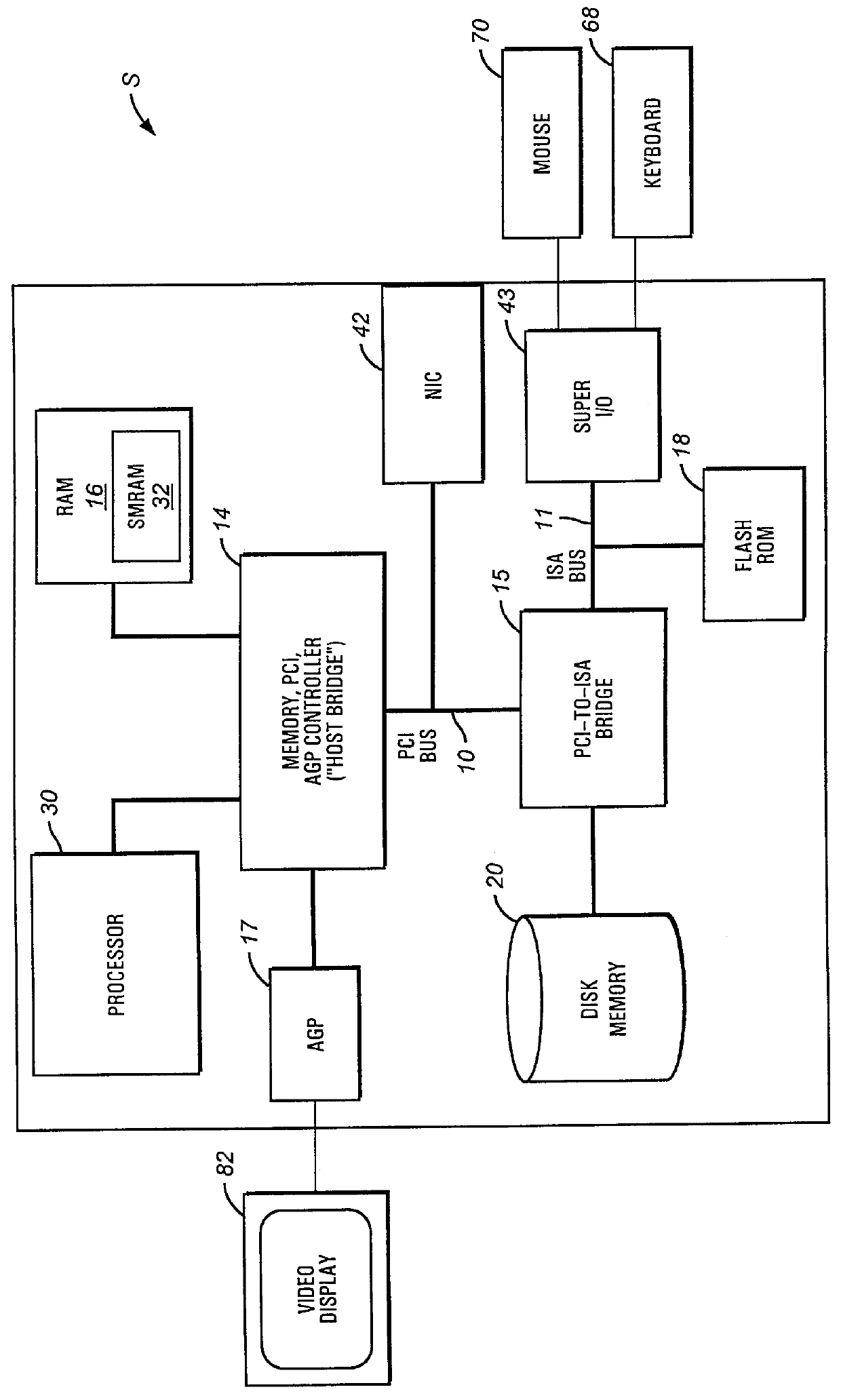
Turning to FIG. 1, illustrated is a typical computing system S according to the present invention. The computing system S in the illustrated embodiment is a PCI bus based machine, having a peripheral component interconnect (PCI) bus 10. The PCI bus 10 is controlled by PCI controller circuitry located within a memory / accelerated graphics port (AGP) / PCI controller 14. This controller 14 (the "host bridge") couples t...


PUM


Abstract

A computing system provides a process for updating a management information format (MIF) database while a processor is operating in a protected mode. The BIOS accesses a protected memory space by utilizing a system management interrupt (SMI). A SMI causes the computing system to enter a system management mode (SMM) and call a Basic Input Output System (BIOS) function, such as the BIOS function 52h (Set Structure), to accomplish an update of the MIF database. An OEM string, for example, may be updated. In SMM, the system is capable of accessing the entire memory address space without risking a memory protection fault.

Description

1. Field of the InventionThe present invention relates generally to a method of updating protected memory areas of a computing system while a processor is in a protected mode and, more particularly, to a method for updating a Desktop Management Interface / System Management Basic Input / Output System (DMI / SMBIOS) portion of flash read-only memory (ROM) of a computing system using a Basic Input / Output System BIOS function 52h (Set Structure) call and a system management interrupt (SMI).2. Description of the Related ArtIn the past decade, the computer industry has grown with breathtaking speed. Not only have the number and types of computers grown exponentially, but also new computer configurations, software products and peripheral devices have proliferated.In parallel with, and perhaps as the result of, the increase of computers, the amount of accessible information has also exploded. As a result, there is a corresponding need for computers to share information and so, increasingly, com...

Claims


Application Information

Patent Timeline
IPC IPC(8): G06F12/14G06F9/445
CPCG06F8/65G06F12/1491G06F2211/1097
Inventor AHUJA, SANJAY
Owner HEWLETT PACKARD DEV CO LP
Learn More