

Wafer-to-wafer transfer of microstructures using break-away tethers
a technology of breakaway tethers and microstructures, applied in the direction of instruments, semiconductor/solid-state device details, charge manipulation, etc., can solve the problem of synergistic fastening mechanisms
- Summary
- Abstract
- Description
- Claims
- Application Information
AI Technical Summary
Benefits of technology
Problems solved by technology
Method used
Image

Examples
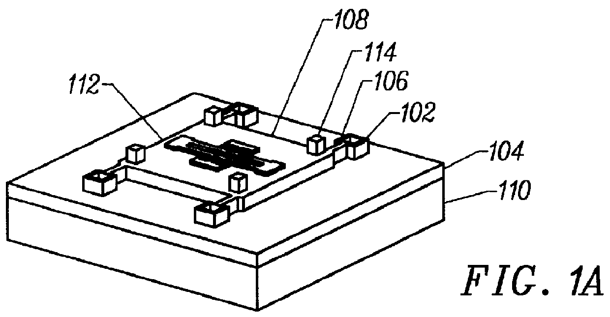
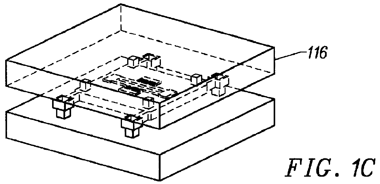
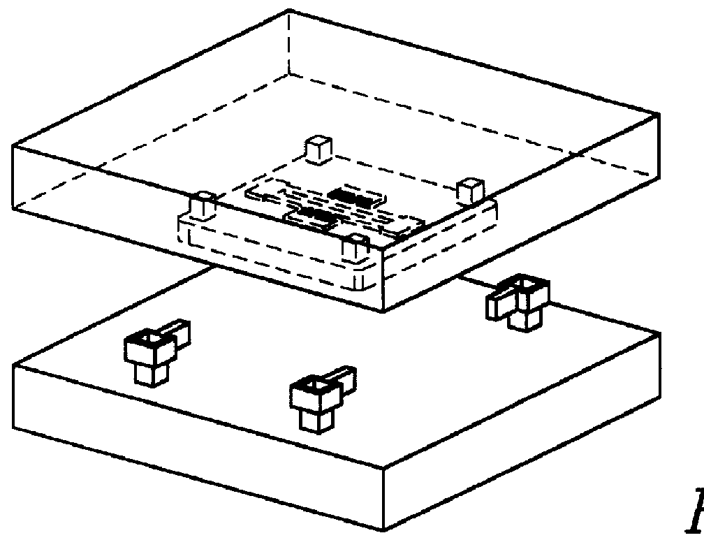
embodiment # 1
Alternate Embodiment #1:FIG. 4--Mechanical Snap Fasteners
FIG. 4 shows an alternate embodiment of the invention, in which mechanical latch or snap mechanisms are employed in place of solder bumps to accomplish the transfer of the chiplet. Each snap mechanism comprises a barb 406, which engages a pair of latches 404. An advantage of the tether structure becomes evident here: its thickness, composition, and shape may be precisely specified, since it is a thin-film, microlithographically-defined structure. Thus, it may be designed to break at a tension suitable to the mechanical snap mechanism. Such snap mechanisms are typically weaker than soldered connections. Another advantage is that the tether may comply in a spring-like fashion, to allow local self-alignment of individual chiplets during the mechanical latching step.
embodiment # 2
Alternate Embodiment #2:FIG. 5--Film Deposition After Transfer
FIG. 5 shows the chiplet / target substrate assembly with the addition of a deposited film 502. The film may be deposited in a directional manner, as by evaporation or sputtering, to create the encapsulated cavity 508 underneath the chiplet. Note that the assembly has been inverted with respect to FIG. 4. The deposited film covers and overhangs the chiplet 108 in the manner of snow overhanging a roof. The encapsulated cavity retains the ambient conditions of the film deposition, typically high vacuum or inert gas.
Hermetic and vacuum-sealed structures are needed for the packaging of microfabricated resonators. Resonators with high quality factor require a vacuum ambient, but previous approaches, based on discrete packages, have been uneconomical.
embodiment # 3
Alternate Embodiment #3:FIG. 5--Film Deposition Before Transfer
FIG. 6 depicts an alternate embodiment of the invention, in which the deposited film 502 is deposited before transfer, after the chiplet has been brought into contact with the target substrate. This serves to bond the chiplet to the target substrate, without the need for solder bumps or latching mechanisms. However, standoffs 602 may be employed to prevent contact between the target substrate and the microstructure itself.
Since the deposited film secures the chiplet to the target substrate, the design may be extremely simple. Also, the possibility of reflow and cross-contamination between materials is minimized. Feature sizes may also be reduced, since thin-film structures are generally smaller than solder bumps. If desired, the film may be reflowed or alloyed after deposition for increased strength.
The film may also be partially removed by directional etching (plasma etching, ion milling). This would allow access to und...
PUM
| Property | Measurement | Unit |
|---|---|---|
| sizes | aaaaa | aaaaa |
| microstructure size | aaaaa | aaaaa |
| thickness | aaaaa | aaaaa |
Abstract
Description
Claims
Application Information