Substrate holding apparatus for processing semiconductor

a technology of holding apparatus and substrate, which is applied in the direction of coating, chemical vapor deposition coating, metallic material coating process, etc., can solve the problems of corrosion, poor thermal efficiency of early susceptors of this type, and inability to achieve process stability. the effect of corrosion

Inactive Publication Date: 2000-12-12
ASM JAPAN +1
View PDF5 Cites 148 Cited by
  • Summary
  • Abstract
  • Description
  • Claims
  • Application Information

AI Technical Summary

Problems solved by technology

However, cracks can occur on the surface of a conventional anodized susceptor in a plasmatic environment at about 400.degree. C., and this has resulted in a problem in that fluorine based active species penetrate into the cracks and react with aluminum to generate a contaminant.
However, early susceptors of this type had poor thermal efficiency and were not preferable in process stability because semiconductor substrates on such susceptors were heated by radiation heat from a lamp in a room separated from the vacuum reaction chamber.
As a result, corrosion is caused by fluorine active species to generate a contaminant.
Thus, even if the interior of a reaction chamber is cleaned through plasma etching, a new contaminant sticks to the surface of the susceptor.
In this case, since it takes a very long time to remove and clean such an integrated susceptor, the apparatus must be stopped for a long time.
This results in the problem of reduced productivity.
A problem arises also from the viewpoint of cost in that a susceptor made of aluminum nitride having an integrated structure is quite expensive.

Method used


Image

  • Substrate holding apparatus for processing semiconductor
  • Substrate holding apparatus for processing semiconductor
  • Substrate holding apparatus for processing semiconductor

Examples


Embodiment Construction

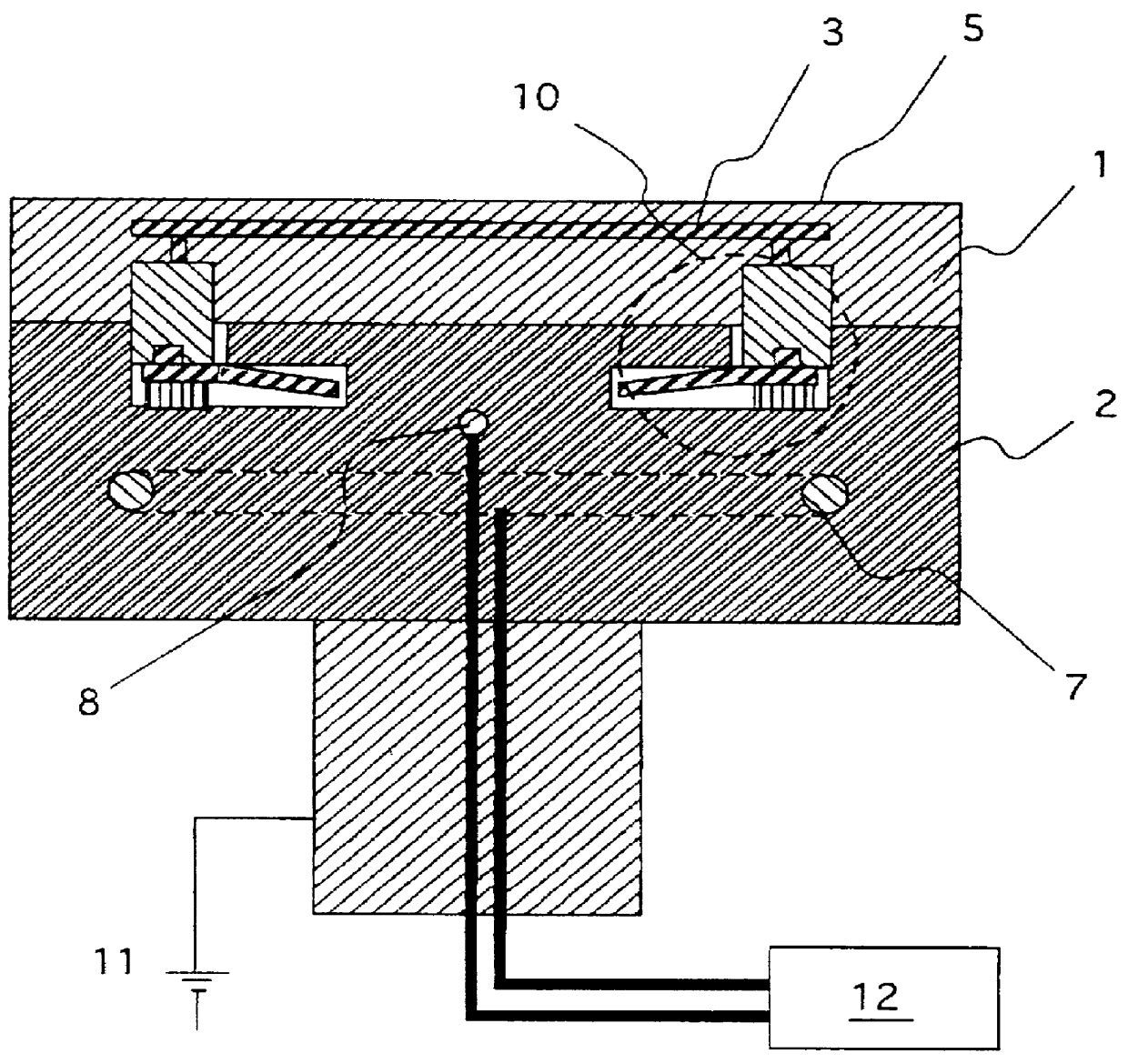
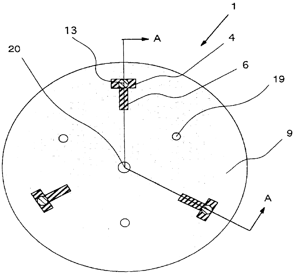
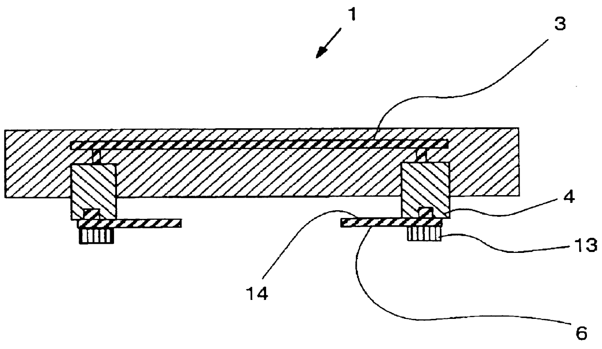
FIG. 1 schematically illustrates a sectional view of a preferred embodiment of a substrate holding apparatus according to the present invention. The substrate holding apparatus of the invention comprises a mount block 1 with a high-frequency electrode 3 embedded therein and having a mount surface 5 for mounting a semiconductor substrate, and a heating block 2 having a heating body 7 embedded therein for heating the semiconductor substrate. Preferably, the mount block 1 is a disc-shaped body having a diameter in the range from 230 mm to 350 mm and a thickness in the range from 3 mm to 9 mm made of aluminum nitride, and the heating block 2 is a cylindrical body having a diameter in the range from 230 mm to 350 mm and a thickness in the range from 20 mm to 100 mm made of aluminum alloy. As described below in detail, the mount block 1 is detachably engaged with the heating block 2 by a lock mechanism 10. A temperature sensor 8 for monitoring the processing temperature of a semiconductor...


PUM

PropertyMeasurementUnit
thicknessaaaaaaaaaa
thicknessaaaaaaaaaa
diameteraaaaaaaaaa

Abstract

A substrate-holding apparatus for holding a semiconductor substrate in a semiconductor processor is characterized in that the apparatus includes a mount block made of, e.g., aluminum nitrate with a high-frequency electrode embedded therein and a heating block made of, e.g., an aluminum alloy with a heating body embedded therein. The mount block is tightly attached to the heating block by engaging the bottom surface of the mount block with the top surface of the heating block, for example, by using a latching mechanism.

Description

1. Field of the InventionThe present invention relates to a substrate holding apparatus for holding a semiconductor substrate in semiconductor processing equipment and, more particularly, to a structure of a susceptor for holding a substrate in plasma CVD equipment.2. Description of the Related ArtConventional susceptors used in plasma CVD equipment comprises an electrode made of aluminum or aluminum alloy which has been anodized on the surface thereof as disclosed in U.S. Pat. No. 5,039,388. This is to provide a susceptor with resistance to fluorine in order to prevent it from generating a contaminant as a result of a reaction with active species in fluorine during plasma etching using a gas including fluorine atoms to clean the interior of the reaction chamber. However, cracks can occur on the surface of a conventional anodized susceptor in a plasmatic environment at about 400.degree. C., and this has resulted in a problem in that fluorine based active species penetrate into the c...

Claims


Application Information

Patent Timeline
Patent Type & Authority Patents(United States)
IPC IPC(8): C23C16/458H01L21/67H01L21/00H01L21/687C23C16/44C23C16/46H01L21/205H01L21/683
CPCC23C16/4581C23C16/4583H01L21/68785H01L21/67103H01L21/68757C23C16/4586
Inventor SATO, KIYOSHISHIMIZU, MIKIOHANAMACHI, TOSHIHIKOMIYAJI, SHINYA
Owner ASM JAPAN
Why Eureka
Try Eureka