Data transfer using two-stage bit switch in memory circuit
- Summary
- Abstract
- Description
- Claims
- Application Information
AI Technical Summary
Benefits of technology
Problems solved by technology
Method used
Image


Examples
Embodiment Construction
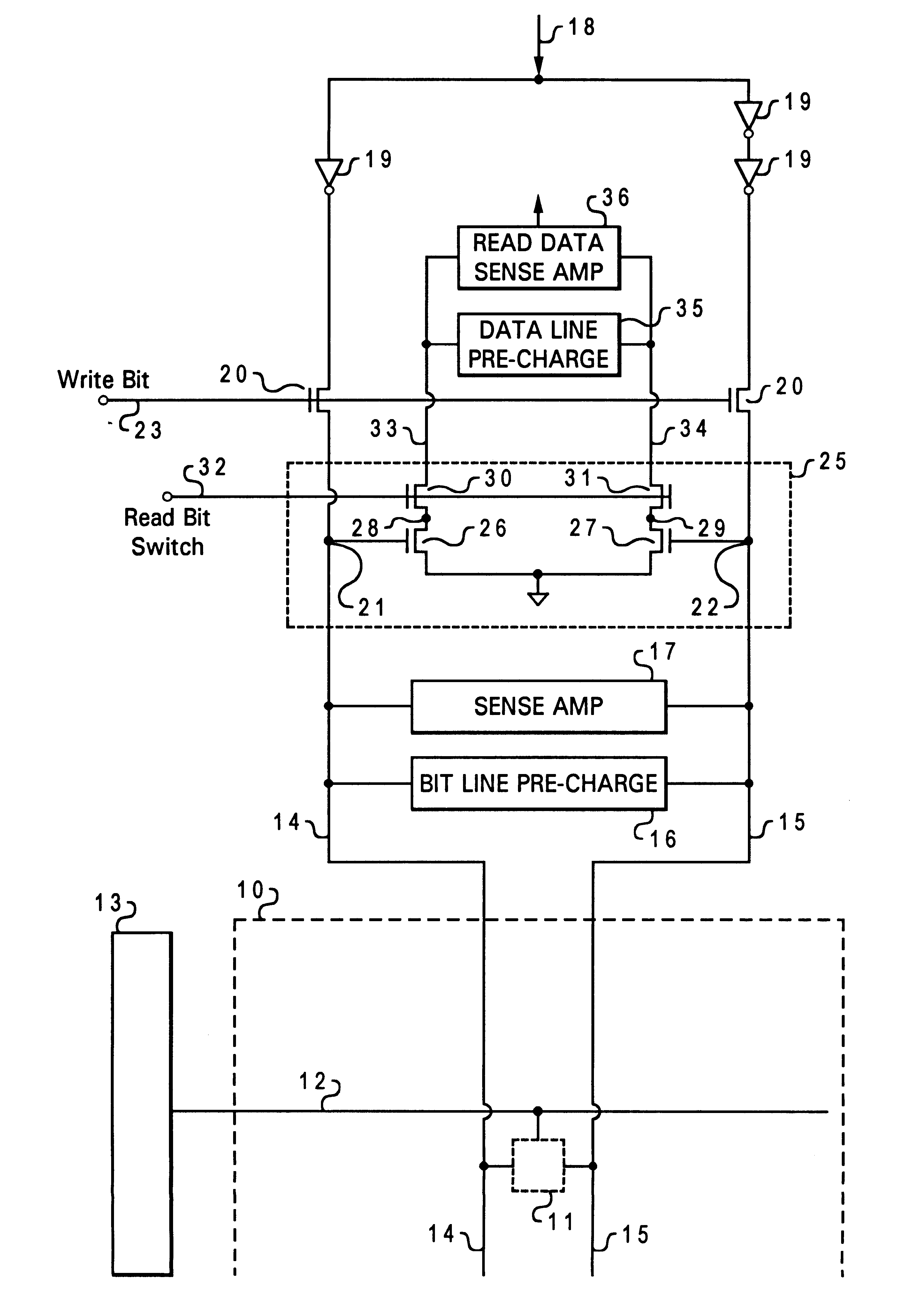
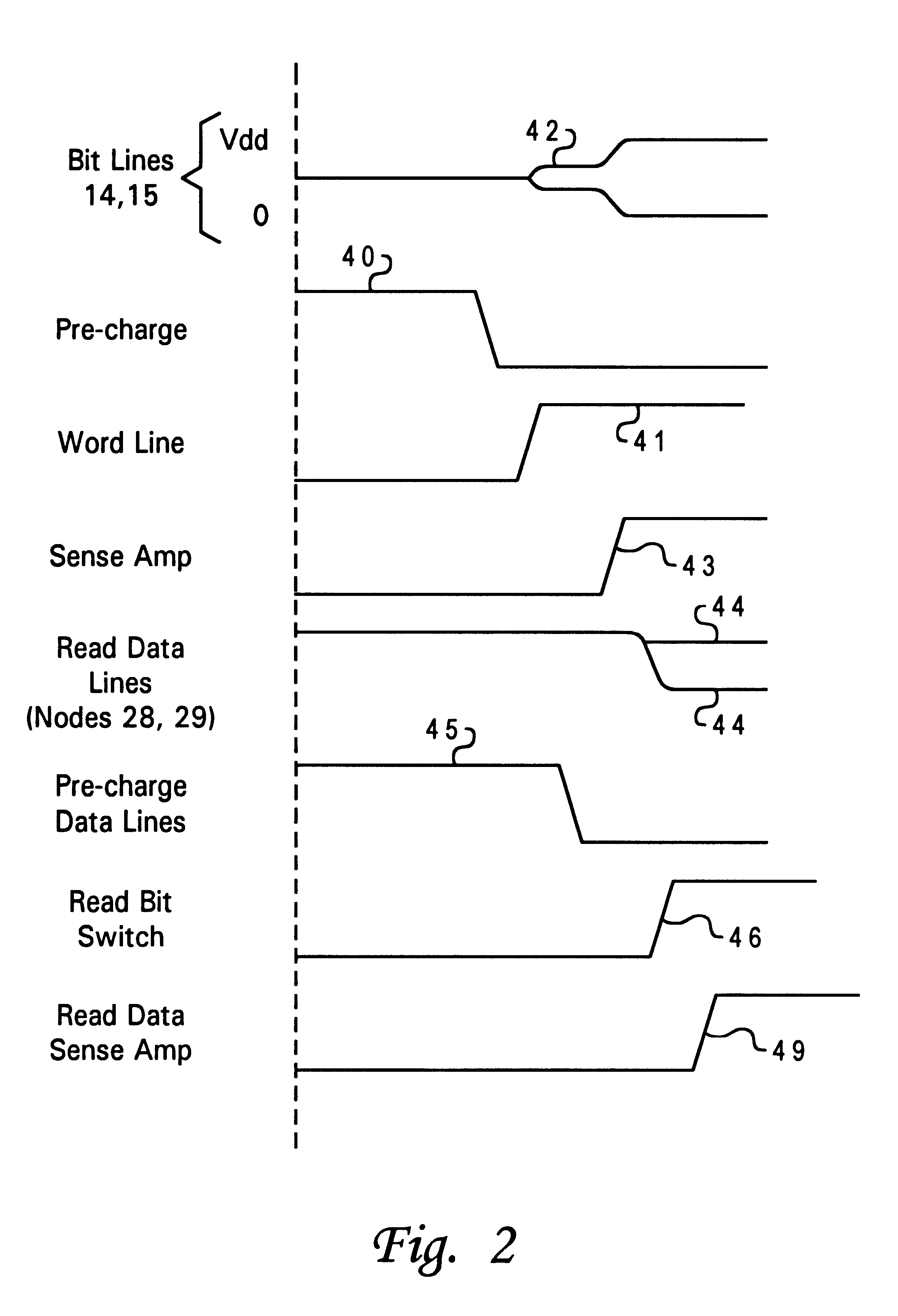
With reference to FIG. 1, a memory circuit is shown employing features of the invention. A memory array 10 formed on a semiconductor chip contains a large number of memory cells 11, in this illustration static memory cells. A word line 12 selects one of the rows of memory cells in the array 10 for read / write operations, based on an address applied to a row decoder 13. Each column of memory cells has a bit line 14 and a complement bit line 15. When selected by the word line 12, one cell in a column will be connected to the bit line pair 14, 15 for writing data into the cell or reading data from the cell.
Connected to the bit line pair 14, 15 for each column of cells is a bit line precharge circuit 16 which functions to precharge the bit line pair 14, 15 to one-half the supply voltage before a read or write cycle. Also connected to each bit line pair in the array 10 is a sense amplifier 17 functioning to detect the slight voltage change on the bit line pair at the initial stage of a re...
PUM
 Abstract
Description
Claims
Application Information
 - R&D Engineer
- R&D Manager
- IP Professional
- Industry Leading Data Capabilities
- Powerful AI technology
- Patent DNA Extraction
Browse by: Latest US Patents, China's latest patents, Technical Efficacy Thesaurus, Application Domain, Technology Topic.
© 2024 PatSnap. All rights reserved.Legal|Privacy policy|Modern Slavery Act Transparency Statement|Sitemap