Integrated cobalt silicide process for semiconductor devices

a cobalt silicide and semiconductor technology, applied in semiconductor devices, thin material processing, electrical equipment, etc., can solve the problems of uneven resistance and leakage of cobalt silicide on the surface of silicon substrate, inconvenient wafer-to-wafer removal, and inability to uniformly remove native oxid

Inactive Publication Date: 2001-02-06
GLOBALFOUNDRIES INC
View PDF7 Cites 24 Cited by
  • Summary
  • Abstract
  • Description
  • Claims
  • Application Information

AI Technical Summary

Benefits of technology

It is also preferred that the apparatus is adapted to provide a constant vacuum and transfer the substrate from the interior chamber adapted to remove oxide from a su

Problems solved by technology

Unfortunately, cobalt silicide formation on the surface of the silicon substrate is not uniform for resistance and leakage across the wafer surface due to the presence of native silicon oxide on the surface of the silicon.
The native oxide may be removed from the substrate by pre-cleaning prior to cobalt deposition, but exposure of the cleaned semiconductor substrate to even low pressure environments results in oxide growth on the cleaned surface in seconds.
In addition, this removal of native oxide is not uniform across the wafer or consistent wafer-to-wafer.
Ex-situ pre-cleaning of the wafer is not a solution because the argon gas used in the device during sputtering occupie

Method used


Image

  • Integrated cobalt silicide process for semiconductor devices
  • Integrated cobalt silicide process for semiconductor devices

Examples


Embodiment Construction

)

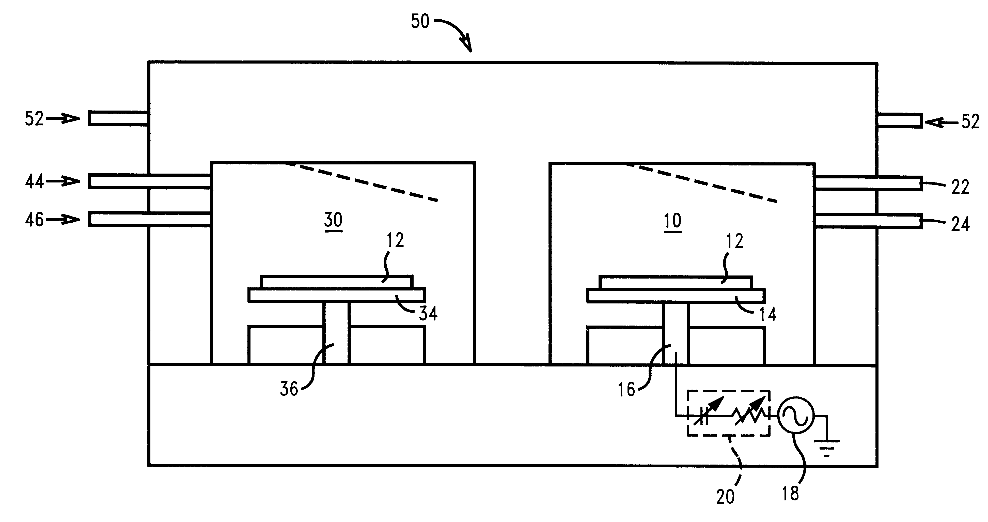
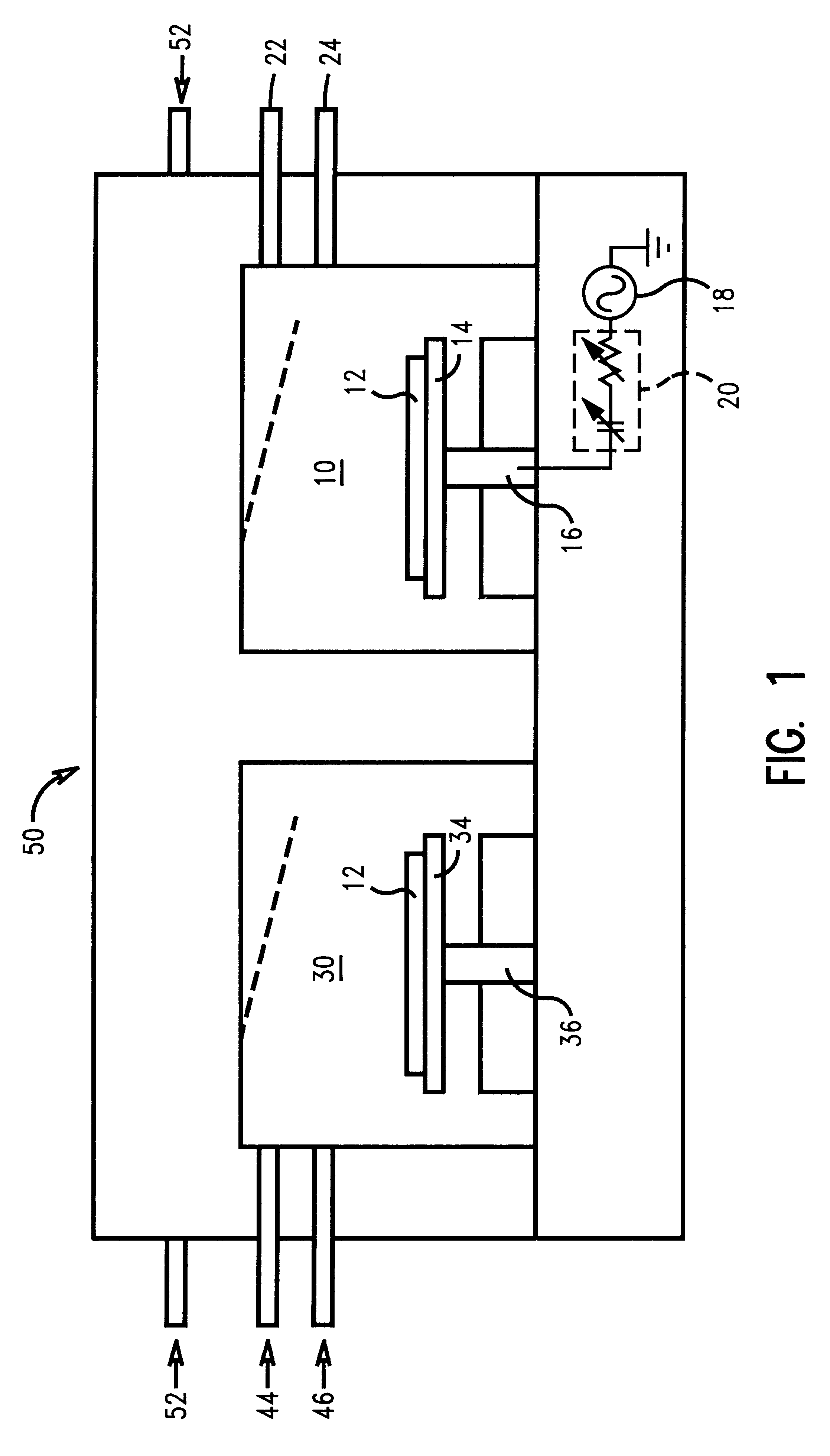
In describing the preferred embodiment of the present invention, reference will be made herein to FIG. 1 of the drawings in which like numerals refer to like features of the invention. Features of the invention are not necessarily shown to scale in the drawing.

It has been found that by eliminating the exposure of a silicon substrate to air after cleaning or removing oxide from the surface of a semiconductor substrate, the probability of native oxide forming on the surface of the silicon substrate is greatly reduced or eliminated. This permits the formation of a uniform silicide layer, such as cobalt silicide, across the surface of the substrate. By integrating the oxide removal process and metal deposition process under a constant vacuum, the cleaned substrate is not exposed to air between steps. In the formation of cobalt silicide, eliminating the exposure to air of the cleaned substrate results in a much more uniform cobalt silicide layer, heretofore not seen in the prior art wit...


PUM


Abstract

A method and apparatus are provided for forming a silicide on a semiconductor substrate by integrating under a constant vacuum the processes of removing an oxide from a surface of a semiconductor substrate and depositing a metal on the cleaned surface without exposing the cleaned surface to air. The method and apparatus of the present invention eliminates the exposure of the cleaned substrate to air between the oxide removal and metal deposition steps. This in-situ cleaning of the silicon substrate prior to cobalt deposition provides a cleaner silicon substrate surface, resulting in enhanced formation of cobalt silicide when the cobalt layer is annealed.

Description

1. Field of the InventionThe present invention relates generally to a method and apparatus for fabricating semiconductor devices and, in particular, to a method and apparatus for forming cobalt silicide on a semiconductor substrate.2. Description of Related ArtOne of the preferred materials useful in forming silicide regions in the fabrication of semiconductor integrated circuits is cobalt. The use of cobalt to form silicide regions is preferred over alternative materials such as titanium and its alloys, platinum or palladium, because cobalt silicide provides low resistivity, allows shallow junctions and lower-temperature processing, and other such advantages.In the prior art, cobalt silicide is formed on a semiconductor device by depositing a layer of cobalt on a silicon substrate and then annealing the cobalt containing surface to form cobalt silicide. Various methods are known in the art for depositing the cobalt on the silicon and include sputtering and evaporation. For convenie...

Claims


Application Information

Patent Timeline
IPC IPC(8): H01L21/285H01L21/02
CPCH01L21/28518Y10S438/906Y10S414/139Y10S438/908
Inventor CANTELL, MARC W.LASKY, JEROME B.LINE, RONALD J.MURPHY, WILLIAM J.PETERSON, KIRK D.TIWARI, PRABHAT
Owner GLOBALFOUNDRIES INC
Why Eureka
Try Eureka