Decoupling capacitor configuration for integrated circuit chip

a technology of integrated circuit chips and capacitors, which is applied in the direction of semiconductor devices, semiconductor/solid-state device details, electrical equipment, etc., can solve the problems of significant power supply voltage excursions, resonance of ac impedance of power supply loop circuits, and increasing the difficulty of power system design

Inactive Publication Date: 2001-02-20
GLOBALFOUNDRIES INC
View PDF27 Cites 68 Cited by
  • Summary
  • Abstract
  • Description
  • Claims
  • Application Information

AI Technical Summary

Problems solved by technology

As high performance integrated circuits demand larger currents at higher frequencies with lower power supply voltages, power system design becomes increasingly challenging.
For example, next generation microprocessors will demand peak currents in excess of 100 A and reach operating frequencies of 1 GHz with power supply voltages below 2 V. At such current levels, surge currents and associated excitations of power distribution system resonances can result in significant power supply voltage excursions.
Unfortunately, in the mid-frequencies (e.g., from approximately 1 MHz to 100 MHz), the AC impedance of the power supply loop circuit is likely to exhibit resonances.
While the impedance at both high- and mid-frequencies can be managed through the use of decoupling capacitors placed strategically in the power supply loop circuit, two significant challenges exist.
First, spatial limitations of an integrated circuit chip can limit the amount of capacitance provided on-die.
Such die footprint can adversely affect die size and yield.
Unfortunately, the inductive impedance of intervening portions of the power supply loop circuit (e.g., of chip and package -level interconnect features such as vias, traces, bonding pads, wires and wire bonds, Tape Automated Bonded (TAB) traces and bonds, solder bumps including Controlled Collapse Chip Connection (C4) bumps, etc.) typically limits the efficacy of off-chip decoupling capacitors.
Unfortunately, even in such configurations, the series inductance from the switching circuits of the integrated circuit to the decoupling capacitance limits the efficacy of the decoupling capacitance.

Method used


Image

  • Decoupling capacitor configuration for integrated circuit chip
  • Decoupling capacitor configuration for integrated circuit chip
  • Decoupling capacitor configuration for integrated circuit chip

Examples


Embodiment Construction

)

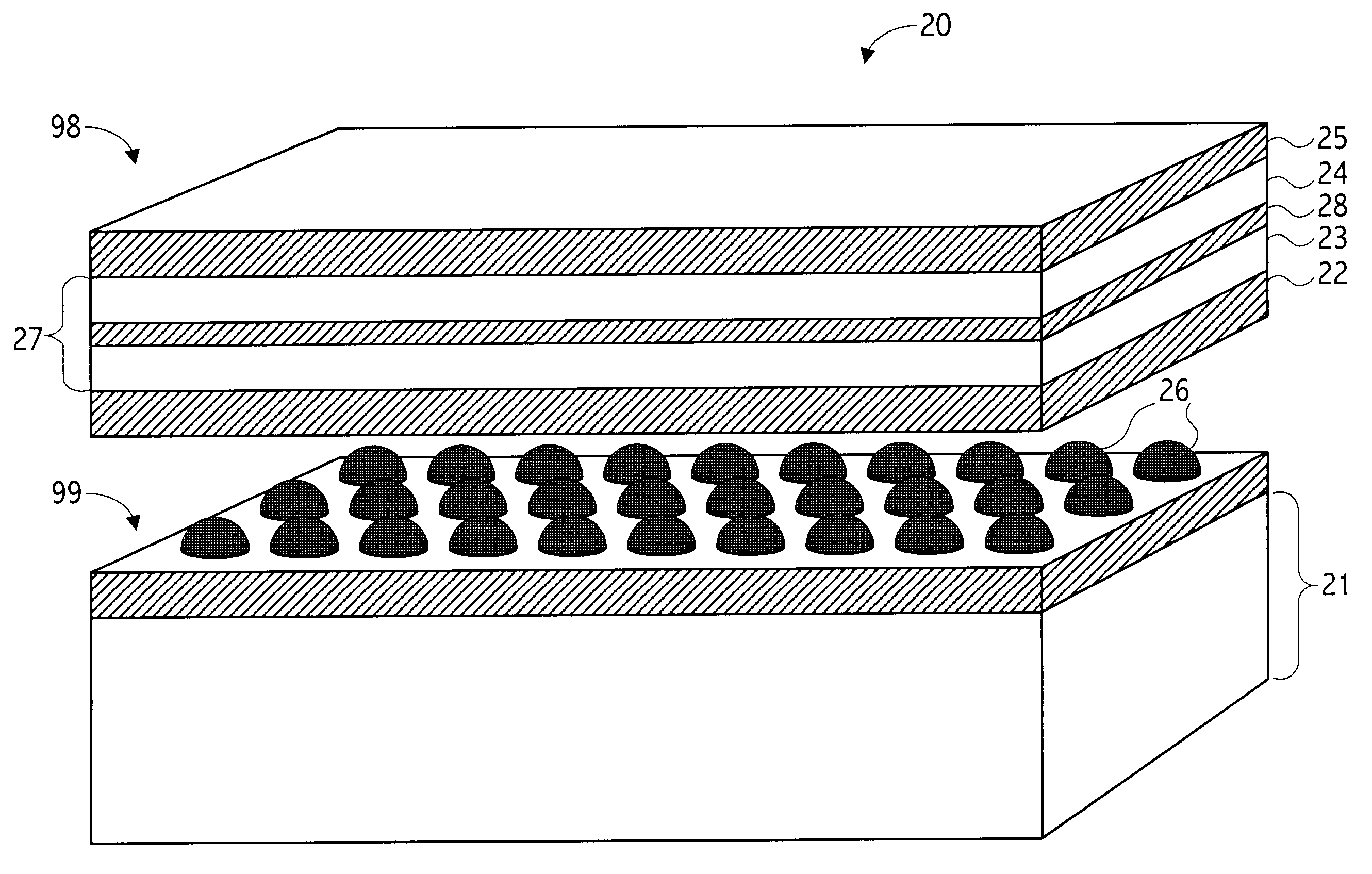
Referring now to FIG. 1, an on-chip decoupling capacitor configuration is shown wherein devices and conductors are defined in a circuitry portion 11 of an integrated circuit chip 10, solder bump connection points (e.g., solder bumps 16) are formed on an upper surface thereof, and a decoupling capacitor 17 is defined between circuitry portion 11 and decoupling capacitor 17. Circuitry defined by semiconductor devices, passives, metal layers, traces, vias, etc. of integrated circuit chip 10 exhibits switching behavior that tends to generate surge currents. Decoupling capacitor 17 stores and supplies charge to satisfy, at least in part, such surge current demands. As further described below, the configuration of FIG. 1 allows the introduction of a large area capacitor in very close electrical proximity to the switching circuits of integrated circuit chip 10. As a result, decoupling capacitor 17 can be effective in mitigating AC voltage noise even for extremely high frequency circuits a...


PUM


Abstract

A decoupling capacitor structure formed integral with an integrated circuit chip and over top of circuitry defined thereon advantageously provides decoupling capacitance in close electrical proximity to switching circuits of the integrated circuit chip without substantially affecting die footprint. In contrast with on-die gate oxide capacitor configurations, a decoupling capacitor structure formed toward the back end of processing, typically after interconnect metal, allows large area capacitor structures without substantial impact on area available for devices and circuitry. Inductance associated with the intervening portion of a power supply loop circuit between switching circuits of the integrated circuit chip and the decoupling capacitor structure can be extremely low in configurations in accordance with the present invention. In some configurations, connection points, e.g., bonding pads and / or solder bumps for conveying power supply voltages, are defined over top of the decoupling capacitor structure.

Description

1. Field of the InventionThis invention relates to power distribution system design, and in particular to managing disturbances otherwise caused by time varying current demands in an integrated circuit.2. Description of the Related ArtAs high performance integrated circuits demand larger currents at higher frequencies with lower power supply voltages, power system design becomes increasingly challenging. For example, next generation microprocessors will demand peak currents in excess of 100 A and reach operating frequencies of 1 GHz with power supply voltages below 2 V. At such current levels, surge currents and associated excitations of power distribution system resonances can result in significant power supply voltage excursions. Accordingly, reductions in the AC impedance of a power distribution system, particularly inductive components thereof, are desired.A variety of techniques are available to improve the AC impedance characteristics of a power distribution system. One such t...

Claims


Application Information

Patent Timeline
Patent Type & Authority Patents(United States)
IPC IPC(8): H01L23/522H01L23/528H01L23/52
CPCH01L23/5223H01L23/5286H01L2924/3011H01L2924/0002H01L2924/00
Inventor HERRELL, DENNIS J.BOETTCHER, MATHIAS
Owner GLOBALFOUNDRIES INC
Why Eureka
Try Eureka