Photoconductive switch with multiple layers

a photoconductive switch and multiple layer technology, applied in the direction of logic circuits, pulse techniques, instruments using specific components, etc., can solve the problems of inability to reduce the contact resistance, the difficulty of obtaining a good contact with a low, and the inability to use sno.sub.2 in the way mentioned abov

Inactive Publication Date: 2001-02-27
ABB (SCHWEIZ) AG
View PDF17 Cites 6 Cited by
  • Summary
  • Abstract
  • Description
  • Claims
  • Application Information

AI Technical Summary

Problems solved by technology

A common problem of such photoconductive switches being irradiated from the same side as one of the contact layers, so-called vertical switches, is the difficulty to obtain a good contact with a low contact resistance on the side of the irradiation and at the same time an efficiently high generation of free charge carriers in the first layer by the irradiation.
It is no practical solution to make the apertures very large and accordingly the contact layer portions separated by said apertures very small, since this will reduce the active area, i.e. the area which may be reach by charge carriers in the conducting state of the switch, of the switch to much and make a substantial contact resistance contribution to the total resistance of the switch.
Thus, it is not p

Method used


Image

  • Photoconductive switch with multiple layers
  • Photoconductive switch with multiple layers
  • Photoconductive switch with multiple layers

Examples


Embodiment Construction

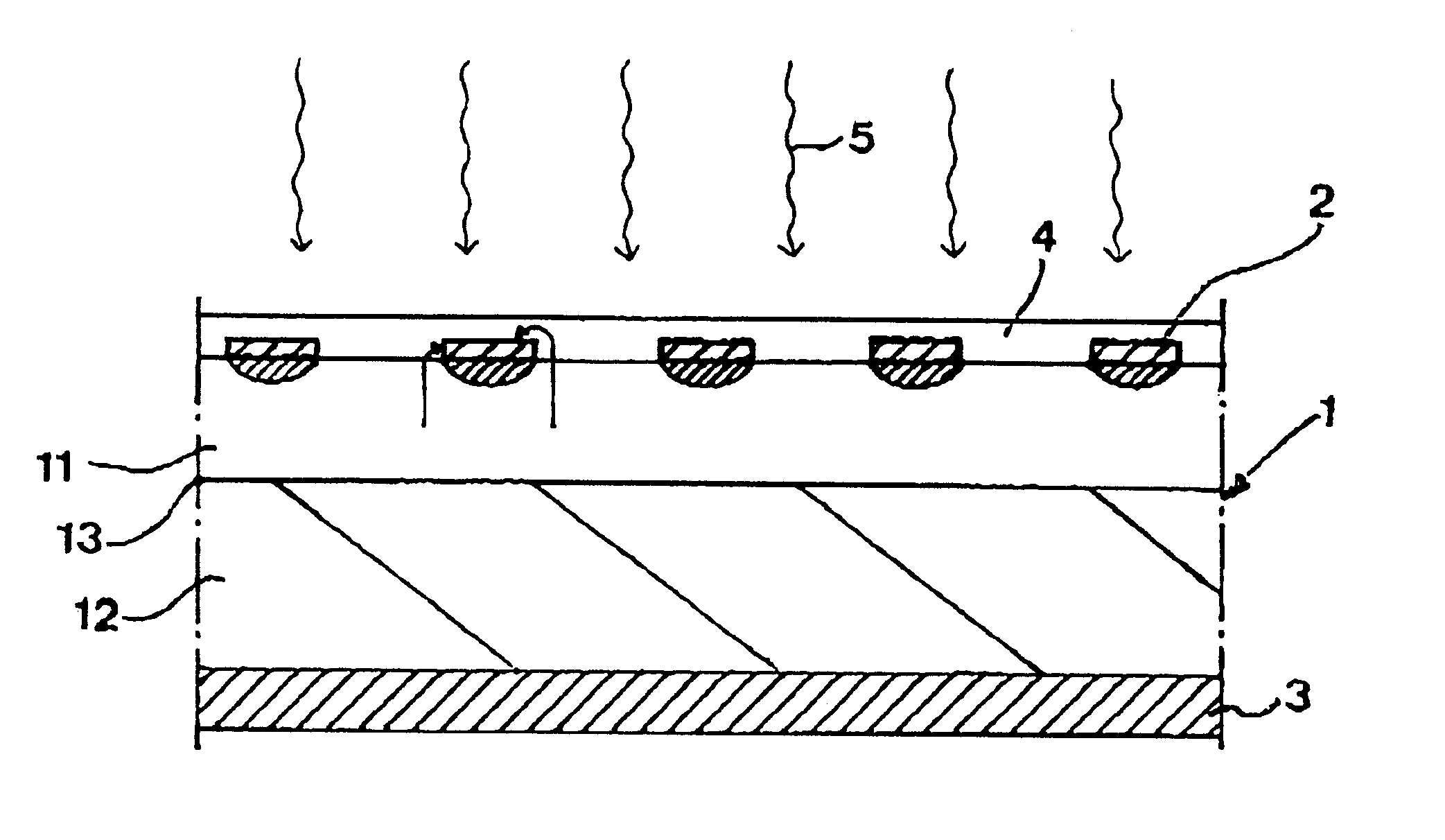
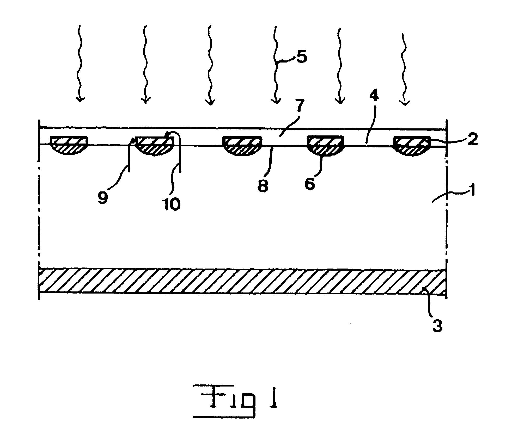
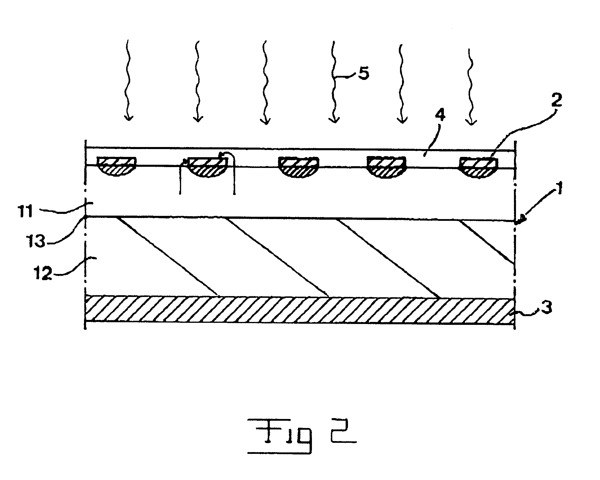
A photoconductive switch according to a preferred embodiment of the invention is very schematically shown in FIG. 1, and this switch has a first layer 1, which in this case is made of intrinsic diamond and typically may have a thickness of about 200 .mu.m, and two contact layers arranged on opposite sides thereof, namely a first contact layer 2 and a second contact layer 3 which are connectable to different potentials for applying a voltage across the first layer 1. Accordingly, the two contact layers are adapted to be connected to an electrode each (not shown) for connecting the switch to for example an electric circuit of an apparatus for controlling a power network.

The first contact layer 2 is provided with apertures 4 allowing light 5 applied on the switch from the side of the first contact layer to reach the first layer for making the switch conducting upon applying a voltage thereacross, irrespectively of the direction of such voltage. The intrinsic diamond of the first layer ...


PUM


Abstract

A photoconductive switch comprises a first layer (1) of a first material sandwiches between two contact layers (2,3). The first layer is adapted to be conducting upon applying a voltage across said contact layers when irradiated by light (5) of an energy high enough for lifting charger carriers from the valence band to the conduction band of the first material. A first (2) of the contact layers is provided with apertures (4) for allowing light applied on the switch to reach said first layer there for making the switch conducting upon applying a voltage across the two contact layers. A thin second layer (7) is arranged on the side of the first contact layers, at least covering the surfaces of the first layer exposed through said apertures and forming an interface to said first layer in said apertures. The second layer is made of a material being able to form a well ordered interface to said first material and having the same or a larger band gap than the latter.

Description

TECHNICAL FIELD OF THE INVENTION AND PRIOR ARTThe present invention relates to a photoconductive switch comprising at least a first layer of a first material and two contact layers arranged on opposite sides of the first layer and connectable to different potentials for applying a voltage across the first layer, said first layer being adapted to be conducting upon applying a voltage across said contact layers when irradiated by light of an energy high enough for lifting charger carriers from the valence band to the conduction band of said first material, a first of said contact layers being provided with apertures for allowing light applied on the switch from the side of said first contact layer to reach said first layer for making the switch conducting upon applying said voltage thereacross.A switch of this type finds many applications, and it may for instance be used in equipment for handling high electric power for switching high voltages (which may be 2-400 kV) and currents, for...

Claims


Application Information

Patent Timeline
IPC IPC(8): H01L31/0264H01L31/08H01L31/0312
CPCH01L31/0312H01L31/08
Inventor BERNHOFF, HANSISBERG, JAN
Owner ABB (SCHWEIZ) AG
Why Eureka
Try Eureka