Direct radiographic imaging panel having a dielectric layer with an adjusted time constant

a dielectric layer and time constant technology, applied in the field of direct radiographic imaging panel, can solve the problems of accumulated charges on the dielectric/photoconductor interface, affecting subsequent exposure of the sensor, and the simplified sensor and transistor structure described above,

Inactive Publication Date: 2001-02-27
DIRECT RADIOGRAPHY
View PDF9 Cites 17 Cited by
  • Summary
  • Abstract
  • Description
  • Claims
  • Application Information

AI Technical Summary

Problems solved by technology

The simplified sensor and transistor structure described above, while quite adequate, is, however, vulnerable to overexposure.
The result of such continuous charge increase is an associated voltage increase on the voltage appearing on the middle electrode which will eventually result in the catastrophic failure of the associated transistor switching element connected to the charge storage capacitor.
While this is an acceptable solution to the overexposure problem, the accumulated charges on the dielectric / photoconductor interface will interfere with subsequent exposures of the sensor.
This extra step is not only time consuming, but, for the reasons discussed later, inhibits the use of this type of sensor for continuous, real time imaging, such as in fluoroscopy applications.

Method used


Image

  • Direct radiographic imaging panel having a dielectric layer with an adjusted time constant
  • Direct radiographic imaging panel having a dielectric layer with an adjusted time constant
  • Direct radiographic imaging panel having a dielectric layer with an adjusted time constant

Examples


example

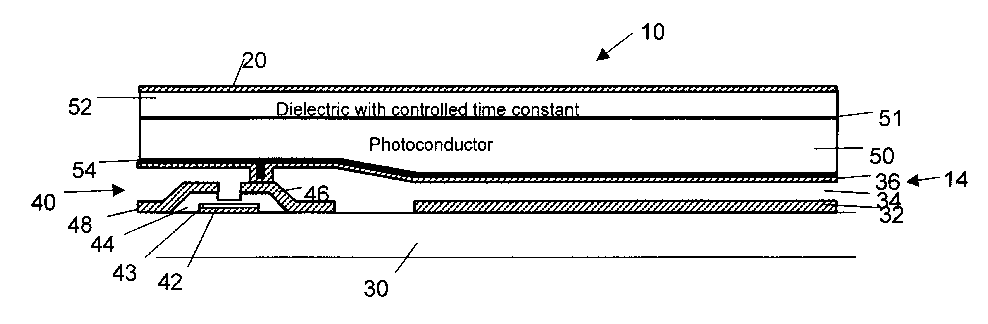
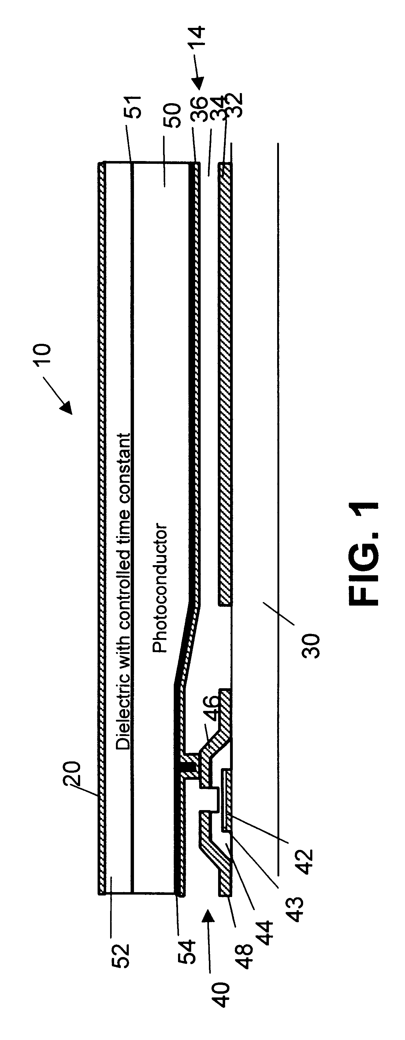
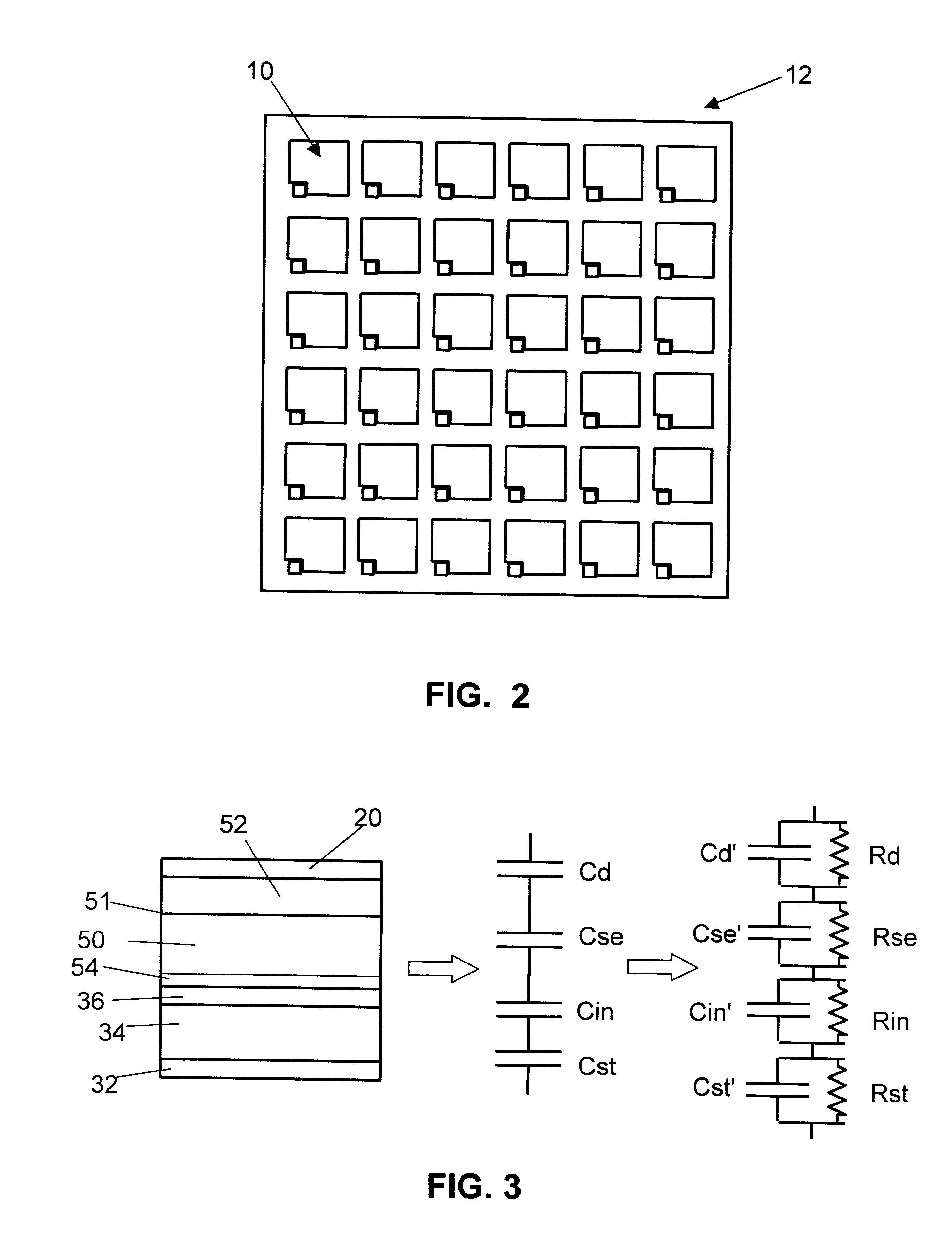
A panel useful for both radiographic and fluoroscopic examinations, comprising an array of a plurality of detectors was constructed by depositing an array of a plurality of first microplates on a glass substrate and by building a TFT switching transistor in a space adjacent each of the microplates. Connecting leads, as needed, were placed between the microplates connecting the drain and gates of the TFT to connection points along the panel sides. Additional leads were placed to provide electrical access to the first microplates. A dielectric layer was placed over the plurality of first microplates, leads and TFTs, and a second plurality of microplates was deposited thereover to produce a TFT module. A passivation layer was created over the middle microplate to act as a unidirectional charge blocking layer and prevent direct electrical contact between the microplate and the photoconductive layer to be coated thereon. Finally the TFT source electrode was connected to the middle microp...


PUM


Abstract

A panel for radiation detection having a plurality of sensors arrayed thereon. Each sensor includes a charge storage capacitor, a radiation sensitive layer over the charge storage capacitor and a dielectric layer over the radiation sensitive layer. The dielectric layer has an adjusted resistivity resulting in a time constant τ=rhokappaepsi0 between 0.050 and 20 seconds, wherein kappa is the dielectric constant of the dielectric layer, and epsi0 is the permitivity of free space. The radiation detection layer is a photoconductor, and the dielectric layer is, preferably, a linear segmented polyurethane.

Description

1. Field of the InventionThis invention relates to radiation sensors in general and more particularly to a radiation detection panel comprising a plurality of radiation sensors which include a dielectric layer with adjusted resistivity.2. Description of Related ArtRadiation sensors able to convert incident radiation directly to an electrical charge indicative of the intensity of the incident radiation are known. Typically such sensors comprise a complex structure which includes a bottom and a middle conductive electrode separated by a dielectric to form a charge storing capacitor. A radiation detection layer, which may be a photoconductive layer, is placed over one of the electrodes. Over the photoconductive layer is another dielectric layer and a top electrode over the dielectric layer completes the sensors structure. Charge blocking layers are often provided between the conductive electrodes and the photoconductive layer.A charging voltage is applied between the top electrode and ...

Claims


Application Information

Patent Timeline
Patent Type & Authority Patents(United States)
IPC IPC(8): G01T1/00G01T1/24H01L31/0216H01L31/0272H01L31/0264H01L27/14H01L31/09H01L31/08H01L31/115H01L31/18
CPCH01L27/14676G01T1/16
Inventor LEE, DENNY L. Y.DAVIS, JAMES E.
Owner DIRECT RADIOGRAPHY
Why Eureka
Try Eureka