IC device contactor

a contactor and device technology, applied in the direction of connection contact member materials, coupling device connections, instruments, etc., can solve the problems of increasing the possibility of contact failure, and affecting the stability of electrical connections,

Inactive Publication Date: 2001-03-20
HITACHI ELECTRONICS ENG CO LTD
View PDF3 Cites 55 Cited by
  • Summary
  • Abstract
  • Description
  • Claims
  • Application Information

AI Technical Summary

Benefits of technology

It is another object of the present invention to provide an IC device contactor which is suitable for use in simultaneously testing a large number of IC devices and which can electrically connect the IC devices securely to a socket board by application of a relatively small pressure.
It is still another object of the present invention to provide an IC device contactor which can protect against damages at least apex portions of spherical electrodes of IC devices under test.

Problems solved by technology

Besides, since the electrodes of IC devices are spherical in shape, difficulties are often encountered in maintaining stable electrical connections with the contact elements on the side of the socket board for all of the electrodes.
Especially in case the spherical electrodes on an IC device is formed by solder balls, their surfaces tend to be oxidized and covered with an oxidation film which would increase the possibilities of contact failures all the more.
Due to repeated contact with IC device electrodes under compressive force, the anisotropic conductive sheet of this sort always has a problem of getting worn out or deteriorated prematurely.
Further, the spherical electrodes on IC devices are of a soft metal like solder balls which can be scraped off quite easily when pressed against an anisotropic conductive sheet for contact therewith and may deposit on the latter as solder debris.
Contact failures may result from such solder debris short circuiting the fine conductive wires.
Especially, since fine conductive wires are provided in a high density on the entire surfaces of the anisotropic conductive sheet, short circuiting across adjacently located solder balls is very likely to occur upon connecting IC devices to an anisotropic conductive sheet on which a large amount of solder debris has deposited.
Nevertheless, there has been a problem that the apex portions of the spherical electrodes can be damaged to a material degree if abutted directly against fine conductive wires of an anisotropic conductive sheet.

Method used


Image

  • IC device contactor
  • IC device contactor
  • IC device contactor

Examples


Embodiment Construction

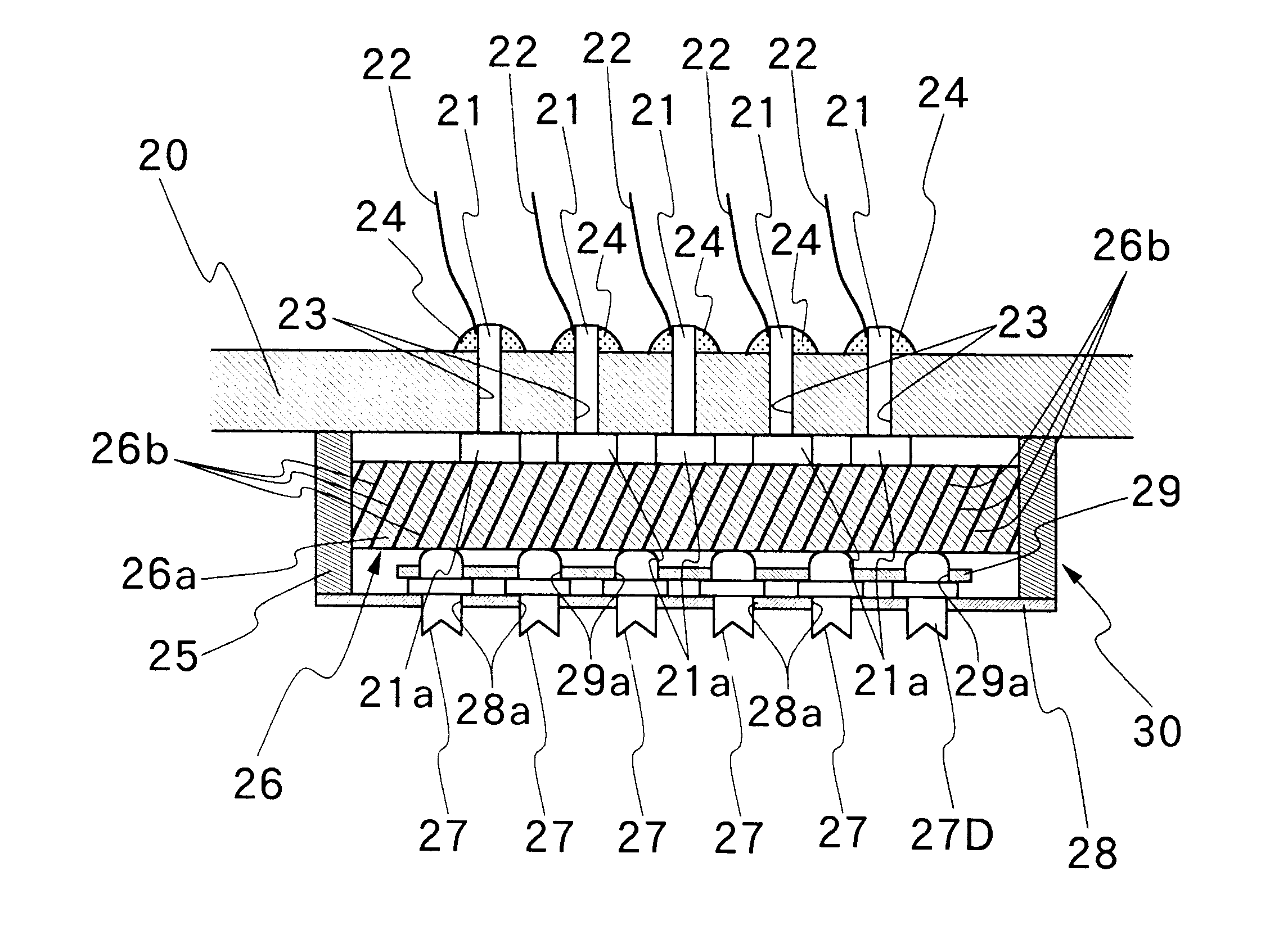
Hereafter, the present invention is described more particularly by way of its preferred embodiment. In the following description, IC devices are connected to a test head under temperature control, using a constant temperature bath to heat or cool IC devices which are mounted on a test board. However, it is to be noted that IC devices can be tested without such temperature control.

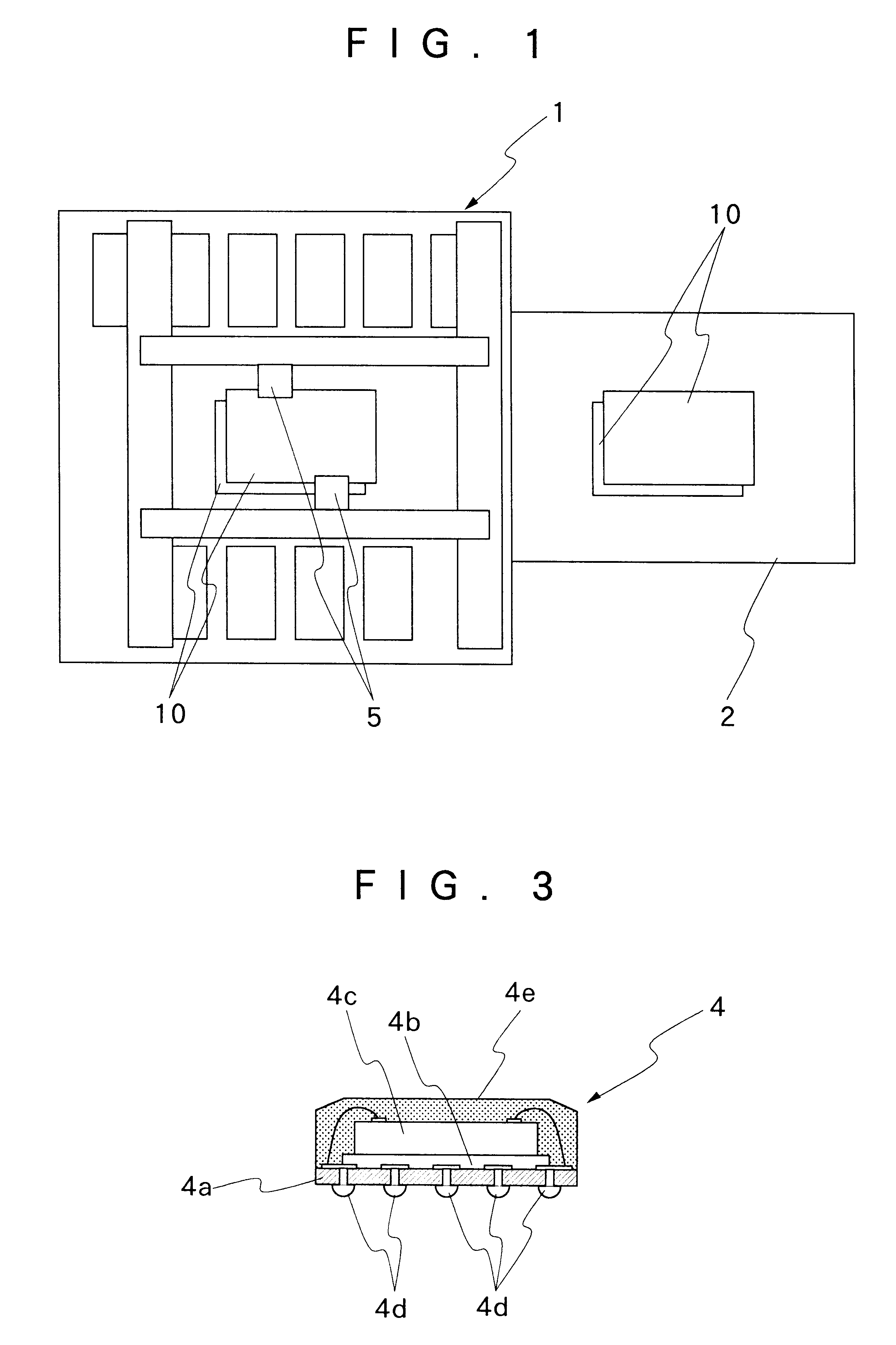
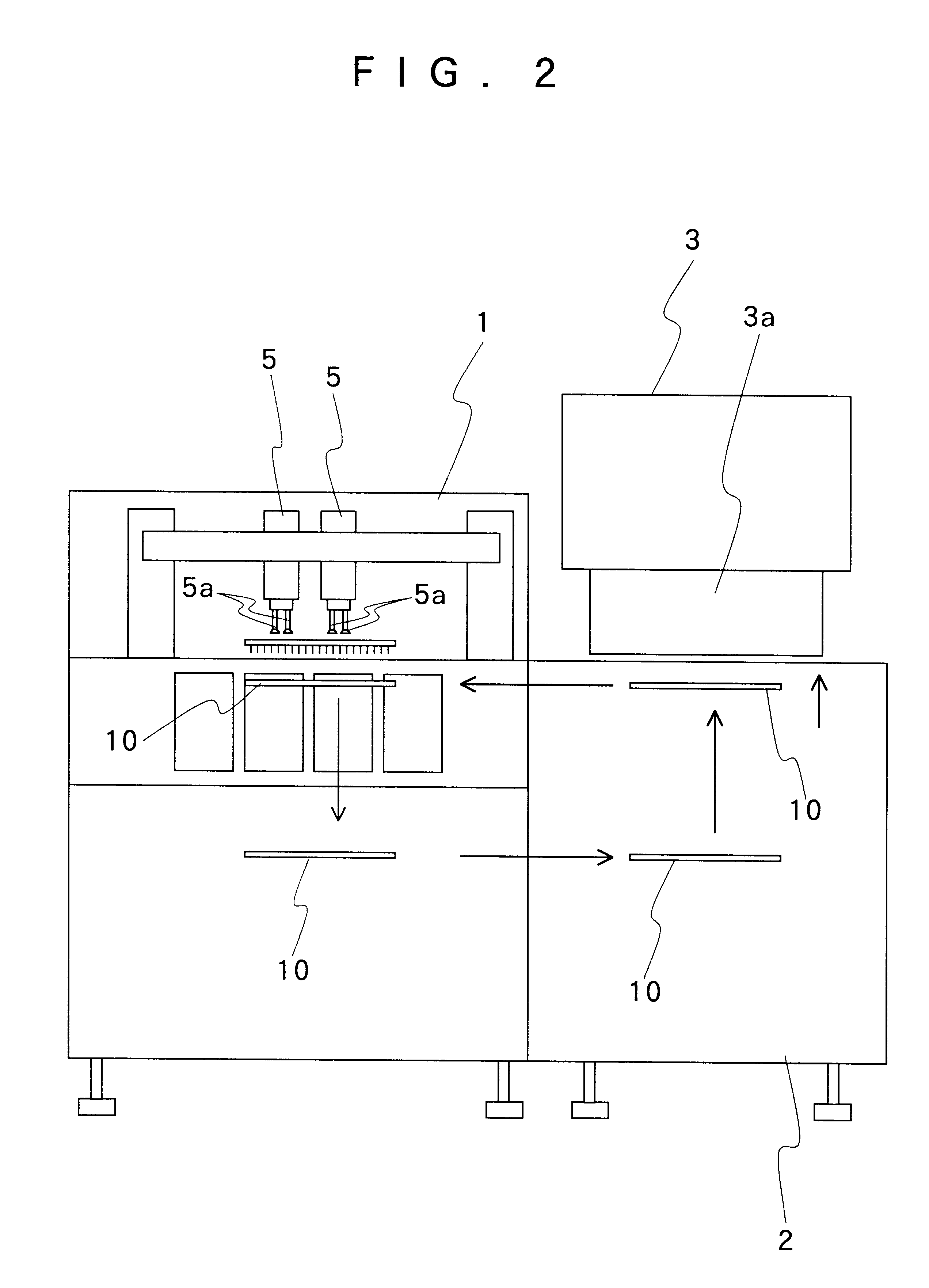
Schematically shown in FIGS. 1 and 2 is the general layout of a typical IC device tester, and in FIG. 3 is an IC device to be tested or measured by the tester.

Referring first to FIGS. 1 and 2, indicated at 1 is a handler, at 2 a constant temperature bath, and at 3 an IC tester. The handler 1 is provided with transfer robots 5 which function to transfer and relocate IC devices, namely, to load and unload IC devices to and from the IC tester. Each transfer robot 5 has suction heads 5a to pick up and transfer IC devices by suction force. By loading and unloading operations by the transfer robots 5, IC devices ...


PUM


Abstract

An IC device contactor for electrically connecting IC devices each having a large number of spherical electrodes on one side of a substrate to an IC tester head for a test of electrical properties or characteristics. The IC device contactor includes: a socket board having a predetermined number of contact points formed on a surface thereof; an anisotropic conductive sheet having a multitude of fine conductive wires embedded in the insulating sheet in an angularly oriented state; a tip holder perforated with a predetermined number of apertures; and a predetermined number of contact tips fitted in the apertures of the tip holder for contact with the spherical electrodes of the IC devices. The anisotropic conductive sheet is disposed with its side in engagement with the socket board and the other side in engagement with the contact tips to electrically connect the contact tips with the contact points on the socket board. The contact tips are assembled with the tip holder in such a way as to be securely retained in position within the respective aperture and are brought into pressed contact with the anisotropic conductive sheet at one end while the other end of the contact tips is projected out of the aperture by a predetermined length.

Description

1. Field of the ArtThis invention relates to an IC device contactor to be used with an IC test machine for electrically connecting thereto spherical electrodes of IC devices, for example, of CSP (chip scale package) type or of BDA (ball grid) type for a test of electrical properties or characteristics.2. Prior ArtIC devices consist of an LSI (large scale circuit) chip with a predetermined number of electrodes. LSI chip are provided as packages shielded in a synthetic resin material. Connected to a large number of electrodes on an LSI chip are lead pins which are generally led out on one side of a package. Lately, however, to comply with demands for IC devices of smaller sizes, there have been developed and put in use IC packages which are reduced almost to the size of an LSI chip and provided with a large number of electrodes substantially of hemispherical shape like solder balls or electrodes of spherical shape arranged in a matrix on a surface on one side of a package instead of l...

Claims


Application Information

Patent Timeline
Patent Type & Authority Patents(United States)
IPC IPC(8): G01R31/28G01R31/26
CPCG01R31/2886H01R33/00
Inventor NAGATSUKA, HIDEAKITAKEUCHI, HIDEYUKIFUKUSHIMA, MAKOTO
Owner HITACHI ELECTRONICS ENG CO LTD
Why Eureka
Try Eureka