
Method of implementing air-gap technology for low capacitance ILD in the damascene scheme

a technology of air gap and damascene, which is applied in the field of implementing air gap technology in the damascene scheme, can solve the problems of limiting the device speed, adding significant delay in the rise and fall of propagating signals, and affecting the chip speed

Inactive Publication Date: 2001-04-10
NOVELLUS SYSTEMS
View PDF5 Cites 109 Cited by
  • Summary
  • Abstract
  • Description
  • Claims
  • Application Information

AI Technical Summary

Benefits of technology

In a second aspect, the present invention relates to a method for implementing low dielectric lines between metal lines in a damascene scheme, comprising the steps of: a) providing a substrate having a substrate top surface; b) polishing the substrate top surface; c) depositing a silicon nitride layer on the substrate top surface; d) forming silicon nitride lines, the nitride lines having exposed top surfaces; e) depositing an oxide layer having an upper surfa

Problems solved by technology

The RC delays associated with the interconnect metal lines of a semiconductor device have become a limiting factor to the speed of the device.
Intra-level line-to-line capacitance increasingly dominates over inter-level capacitance, adding significant delay to the rise and fall times of the propagating signals.
Greater capacitance of the interconnecting material, i.e., a greater dielectric constant, will delay the rise and fall times of signals in the metal lines, thereby adversely affecting the chip speed.
Polymers with dielectric constants on the order of k=2.5 have been used as the interconnecting material, but these materials are unstable under thermal treatment and throughout the chip fabrication process.
However, fluorine is also not stable and will degrade the metal lines that are in contact with it.
However, they are extremely unstable during the fabrication process and are susceptible to shrinkage.
These materials are also known to cause deleterious effects during chemical-mechanical polishing, a necessary process step in chip fabrication.
However, mechanical rigidity and device reliability are compromised with air bridges.
Also, chip to chip variations in device speed and power consumption are prevalent when air bridge gaps are introduced.

Method used


Image

  • Method of implementing air-gap technology for low capacitance ILD in the damascene scheme
  • Method of implementing air-gap technology for low capacitance ILD in the damascene scheme
  • Method of implementing air-gap technology for low capacitance ILD in the damascene scheme

Examples


Embodiment Construction

)

In describing the preferred embodiment of the present invention, reference will be made herein to FIGS. 1-8 of the drawings in which like numerals refer to like features of the invention. Features of the invention are not necessarily shown to scale in the drawings.

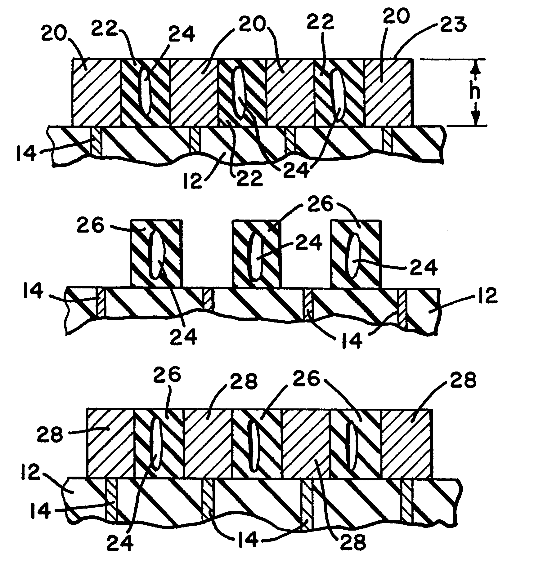
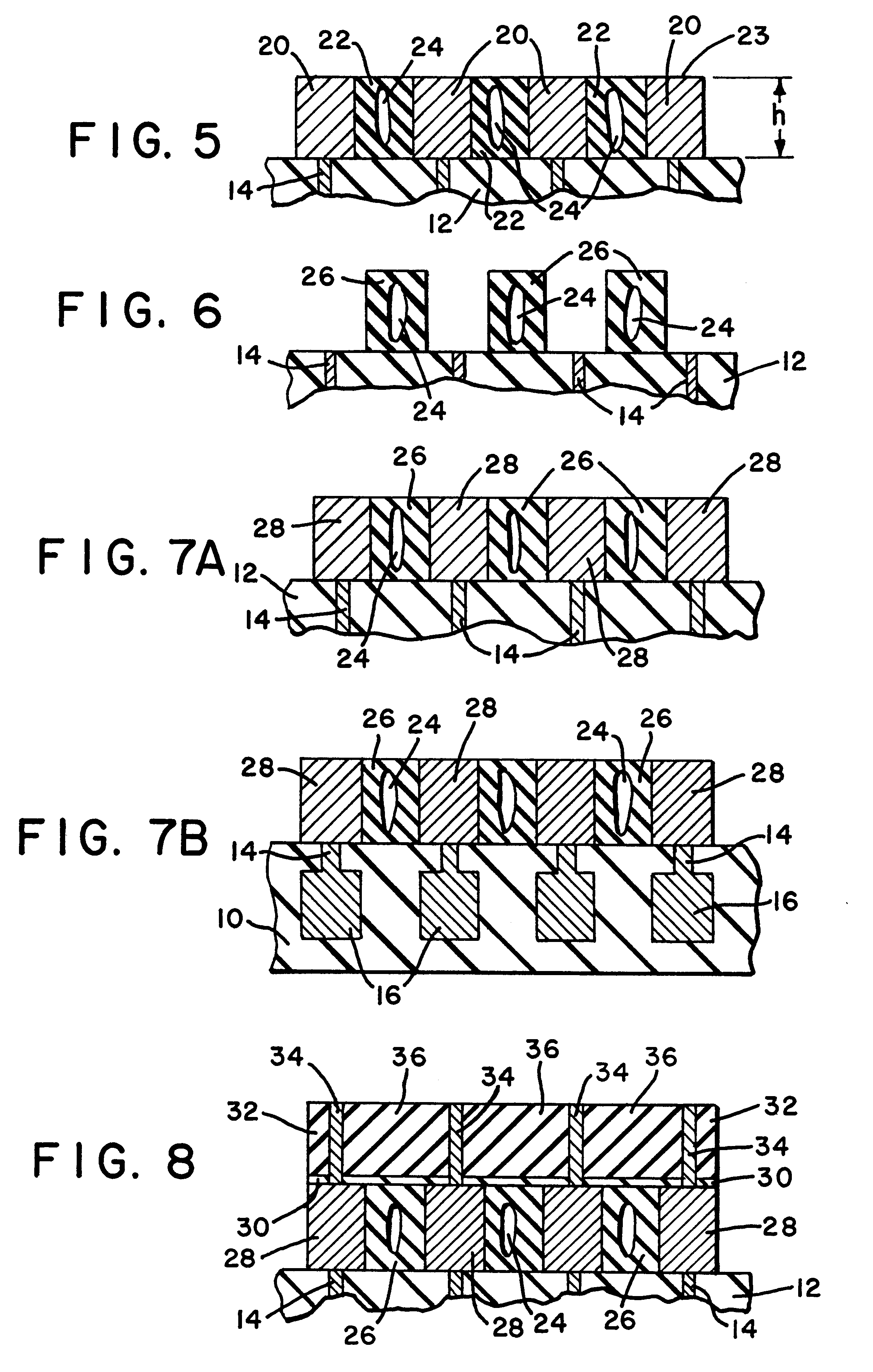
In order to achieve effective k-values as low as 1.9 to 2.5, a controlled air-gap formation is demonstrated in a subtractive aluminum multilevel interconnect structure. The preferred process implementing this technology in the damascene scheme is described herein.

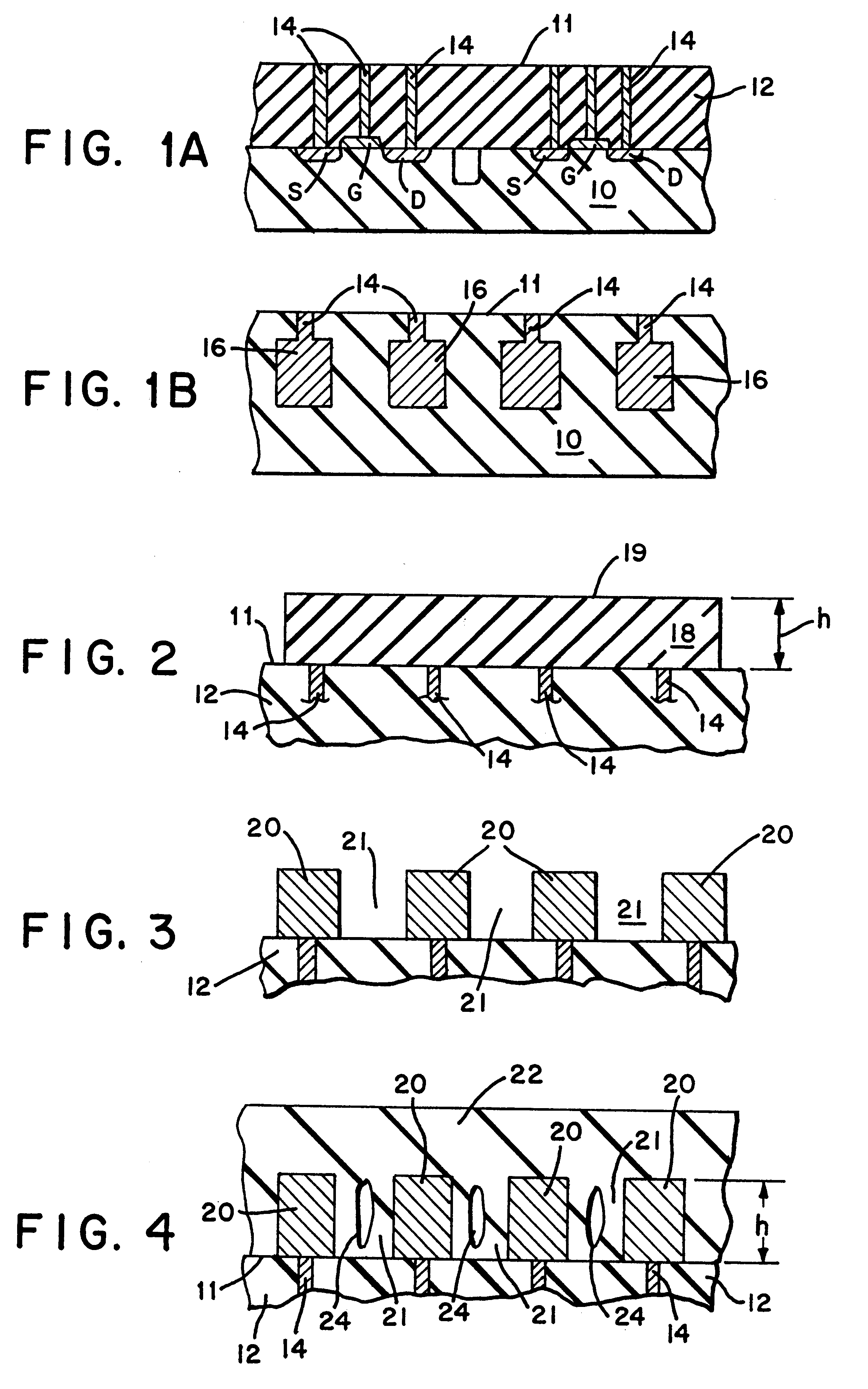
FIG. 1A depicts the starting substrate 10, which is typically the first level of a damascene structure. The substrate may be composed of several dielectric layers of a multi-layer structure (an inter-layer device or ILD). If the substrate is layered, it may have metal connections exposed to provide electrical contact with the next layer to be subsequently configured.

There are two forms for a starting substrate when implementing a process in the damascene scheme (...


PUM


Abstract

Air-gap technology is introduced in the damascene scheme, reducing the capacitance between interconnect metal lines on an integrated circuit substrate, and ultimately enhancing the speed of the device. Reduction of extraneous signal energy (cross-talk) from traversing from one metal line to another is also realized. The method for implementing an air-gap filled dielectric between the interconnect metal lines involves depositing a first dielectric layer on the substrate at a predetermined height. Next the first dielectric is patterned and etched to form lines. A second dielectric layer is then deposited using air-gap technology, such that the second dielectric contains air-gaps between the first dielectric lines. These air-gaps are situated below the predetermined height of the first dielectric. The substrate is then polished so that the top surface of the first dielectric is exposed. The first dielectric lines are then etched and removed. A metal is deposited in place of the removed first dielectric lines, forming interconnect metal lines on the substrate having an air-gap filled dielectric therebetween. The air-gap filled dielectric has a dielectric constant on the order of k=1.9 to 2.5, which is significantly lower than that of the same dielectric material without the air-gap.

Description

1. Field of the InventionThe present invention, in general, relates to a semiconductor process, and more specifically, to a method of implementing air-gap technology in a semiconductor device so as to reduce parasitic capacitance between metal lines, improve the integrated circuit chip speed, and reduce power consumption and cross-talk.2. Description of Related ArtAs device dimensions continue to shrink, the parasitic effects of line to line capacitance becomes a critical factor to performance and circuit integrity. The RC delays associated with the interconnect metal lines of a semiconductor device have become a limiting factor to the speed of the device. Intra-level line-to-line capacitance increasingly dominates over inter-level capacitance, adding significant delay to the rise and fall times of the propagating signals. Reducing the capacitance between the interconnect metal lines on an integrated circuit chip will enhance the speed of the device and reduce extraneous signal ener...

Claims


Application Information

Patent Timeline
IPC IPC(8): H01L21/768H01L21/70
CPCH01L21/7682
Inventor NAG, SOMNATH
Owner NOVELLUS SYSTEMS
Features
  • Generate Ideas
  • Intellectual Property
  • Life Sciences
  • Materials
  • Tech Scout
  • Unparalleled Data Quality
  • Higher Quality Content
  • 60% Fewer Hallucinations
Learn More