Asymmetrical IGFET devices with spacers formed by HDP techniques

a technology of igfet and spacer, which is applied in the direction of semiconductor devices, basic electric elements, electrical equipment, etc., can solve the problems of spacers having unacceptable thickness or unacceptable geometry, and the formation rate of silicon oxide materials and etching rates can be uncertain

Inactive Publication Date: 2001-04-17
GLOBALFOUNDRIES INC
View PDF24 Cites 29 Cited by
  • Summary
  • Abstract
  • Description
  • Claims
  • Application Information

AI Technical Summary

Problems solved by technology

However, this procedure has problems associated therewith.
Both the rate of formation of the silicon oxide material and the etching rate can be uncertain.
This uncertainty can result in spacers having unacceptable thi

Method used


Image

  • Asymmetrical IGFET devices with spacers formed by HDP techniques
  • Asymmetrical IGFET devices with spacers formed by HDP techniques
  • Asymmetrical IGFET devices with spacers formed by HDP techniques

Examples


Embodiment Construction

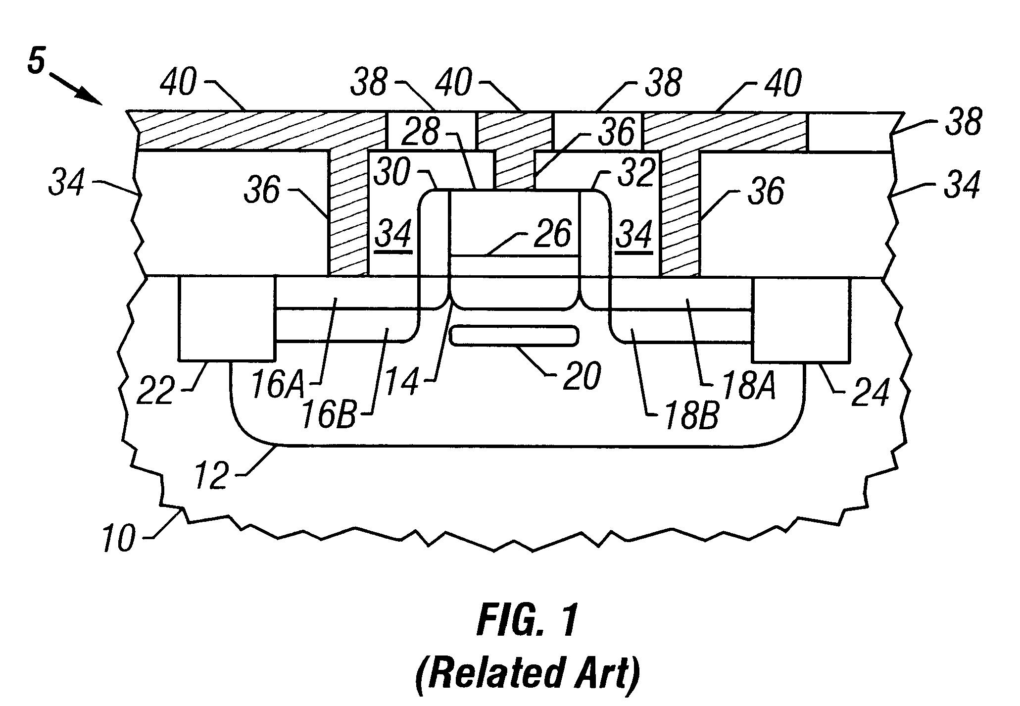
FIG. 1 has been discussed with respect to the related art.

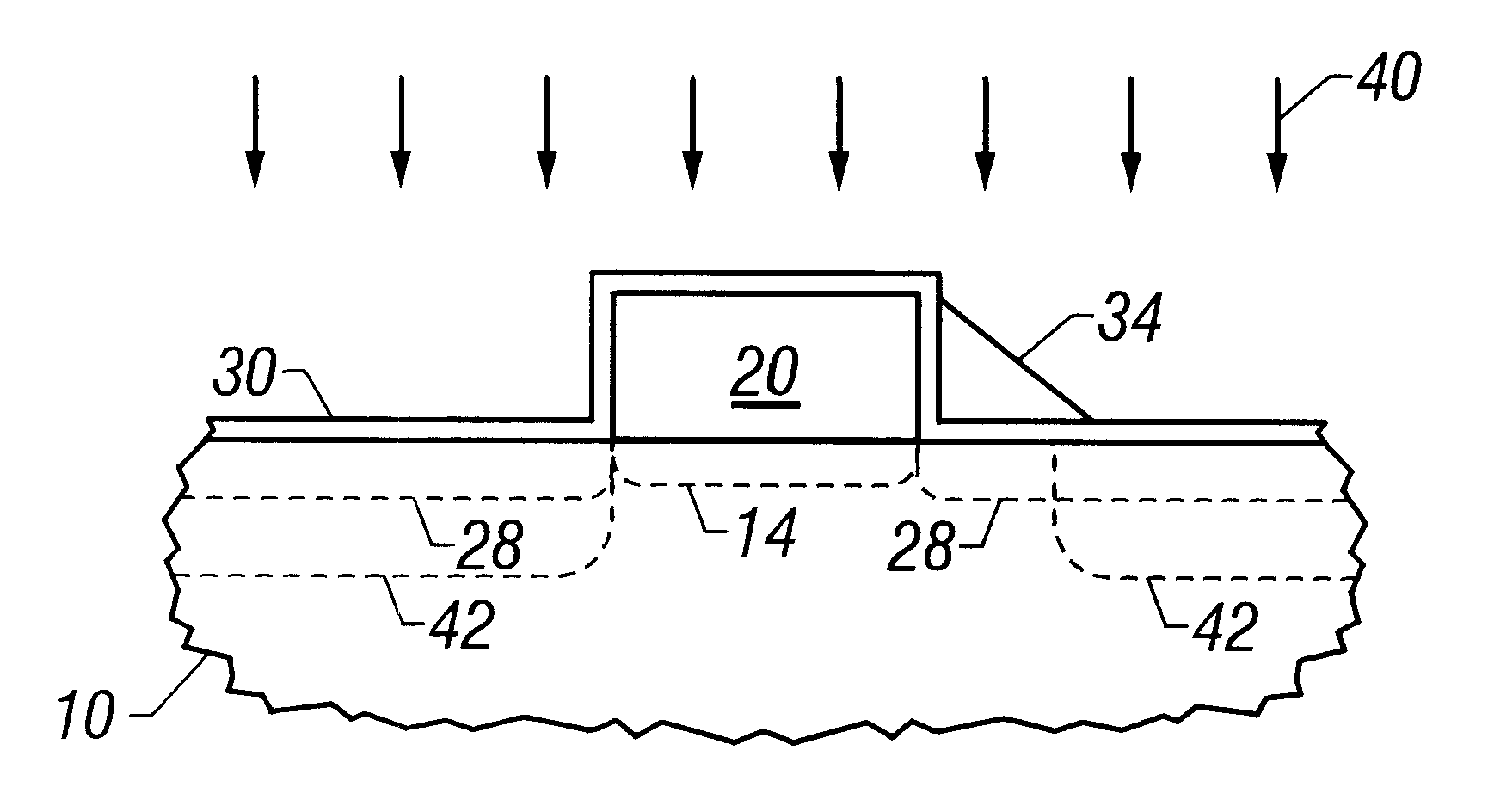
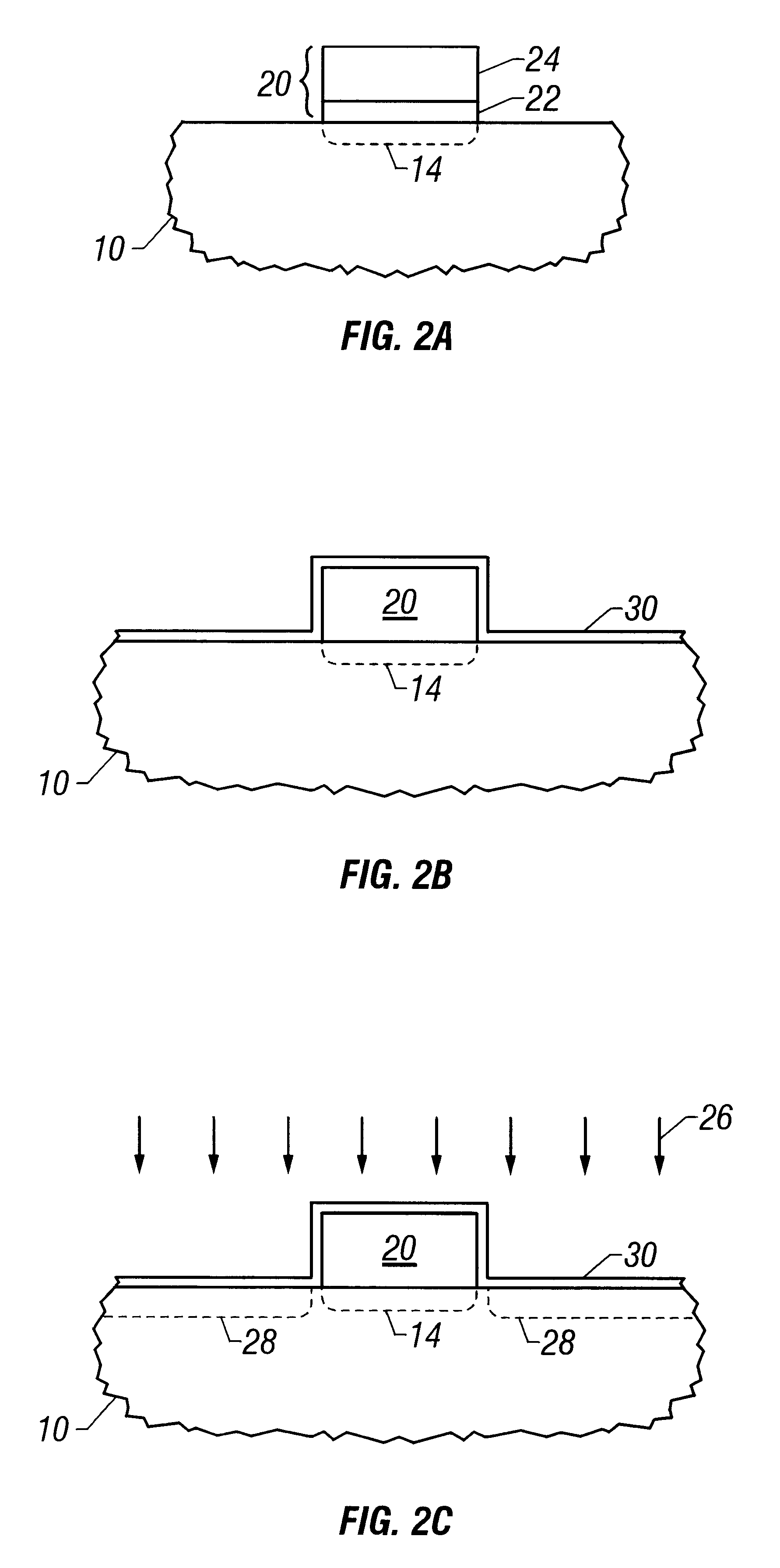
Referring to FIG. 2A, the substrate 10 has a well region (not shown), a punch-through region (not shown), and a channel region 14 formed therein. The channel region 14 can be doped with arsenic ions or phosphorous ions to form an n-doped channel region, an n-doped punch-through region, and an n-doped well region; or can be doped with boron to form a p-doped channel region, a p-doped punch-through region, and a p-doped well region. (For the doping of the source / drain regions, the doping ions are reversed from those forming these regions in the substrate 10.) In order to implant the ions at the desired doping concentration and depth levels, phosphorous is implanted to form a channel region with an approximate energy of 15 to 150 keV with a total ion density of approximately 1.times.10.sup.12 to 1.times.10.sup.13 ions / cm.sup.2 ; is implanted to form a punch-through region with an approximate energy of 75 to 225 keV with a total ...


PUM


Abstract

In an IGFET device having at least one source/drain region with a lightly-doped sub-region proximate a channel region, the source/drain regions are formed by first implanting ions with parameters to form lightly-doped source/drain regions. A high density plasma deposition provides at least one spacer having preselected characteristics. As a result of the spacer characteristics, an ion implantation with parameters to form normally-doped source/drain regions is shadowed by the spacer. A portion of the source/drain region shadowed by the spacer results in a lightly-doped source/drain sub-region proximate the channel region. According to a second embodiment of the invention, the ion implantation resulting in the lightly-doped source/drain regions is eliminated. Instead, the spacer(s) formed by the high density plasma deposition and subsequent etching process only partially shadows the ion implantation that would otherwise result in normal doping of the source/drain regions. The parameters of the spacer(s) resulting from the high density plasma deposition and subsequent etching process result in a lightly-doped source/drain sub-region proximate the channel region. The shadowing of the spacer decreases with distance from the gate structure and results in a normal doping level for the portion of the source/drain terminal not shadowed by the spacer.

Description

1. Field of the InventionThis invention relates generally to the fabrication of integrated circuits and, more particularly to the fabrication of insulated gate, field effect transistor (IGFET) devices. This invention is related specifically to (IGFET) devices that have source / drain regions having two sub-regions, each sub-region with a different doping level.2. Description of the Related ArtAn insulated gate, field effect transistor (IGFET) device 5, such as a metal-oxide semiconductor field-effect transistor (MOSFET) is shown in FIG. 1. A substrate 10 has a doped well region 12, a p-doped well region that will be used for purposes of illustration. The substrate 10 has a p-doped channel region 14 that provides a conducting path between the n-doped source / drain region 16A, 16B and the n-doped source / drain region 18A, 18B. In addition, a p-doped punch-through region 20, is provided below the channel region 14. Also formed in the substrate 10 are the isolation structures 22 and 24. The...

Claims


Application Information

Patent Timeline
IPC IPC(8): H01L21/336H01L21/02H01L29/66H01L29/78
CPCH01L29/6653H01L29/66598H01L29/66659H01L29/7835
Inventor KADOSH, DANIELGARDNER, MARK I.
Owner GLOBALFOUNDRIES INC
Why Eureka
Try Eureka