Die bonding apparatus

a technology of die-bonding and sintering rods, which is applied in the direction of solventing equipment, manufacturing tools, transportation and packaging, etc., can solve the problems of not being used and left with the equipmen

Inactive Publication Date: 2001-05-01
SAMSUNG ELECTRONICS CO LTD
View PDF7 Cites 25 Cited by
  • Summary
  • Abstract
  • Description
  • Claims
  • Application Information

AI Technical Summary

Problems solved by technology

In addition, there is a drawback that the facilities are left and not used because the

Method used


Image

  • Die bonding apparatus
  • Die bonding apparatus
  • Die bonding apparatus

Examples


Embodiment Construction

Reference will now be made in detail to the preferred embodiments of the present invention, examples of which are illustrated in the accompanying drawings.

With reference to the accompanying drawings, the present invention will now be described in detail.

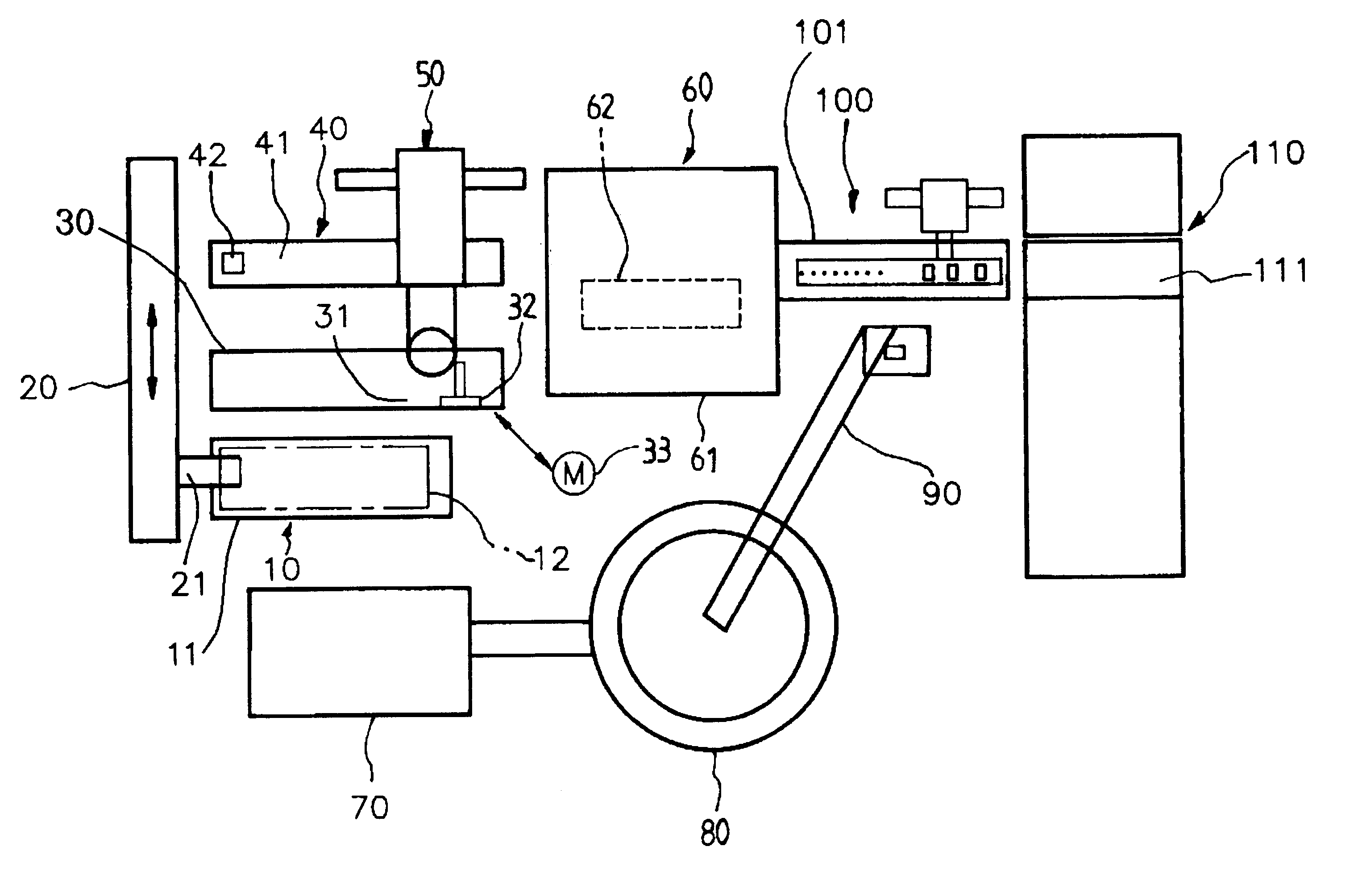
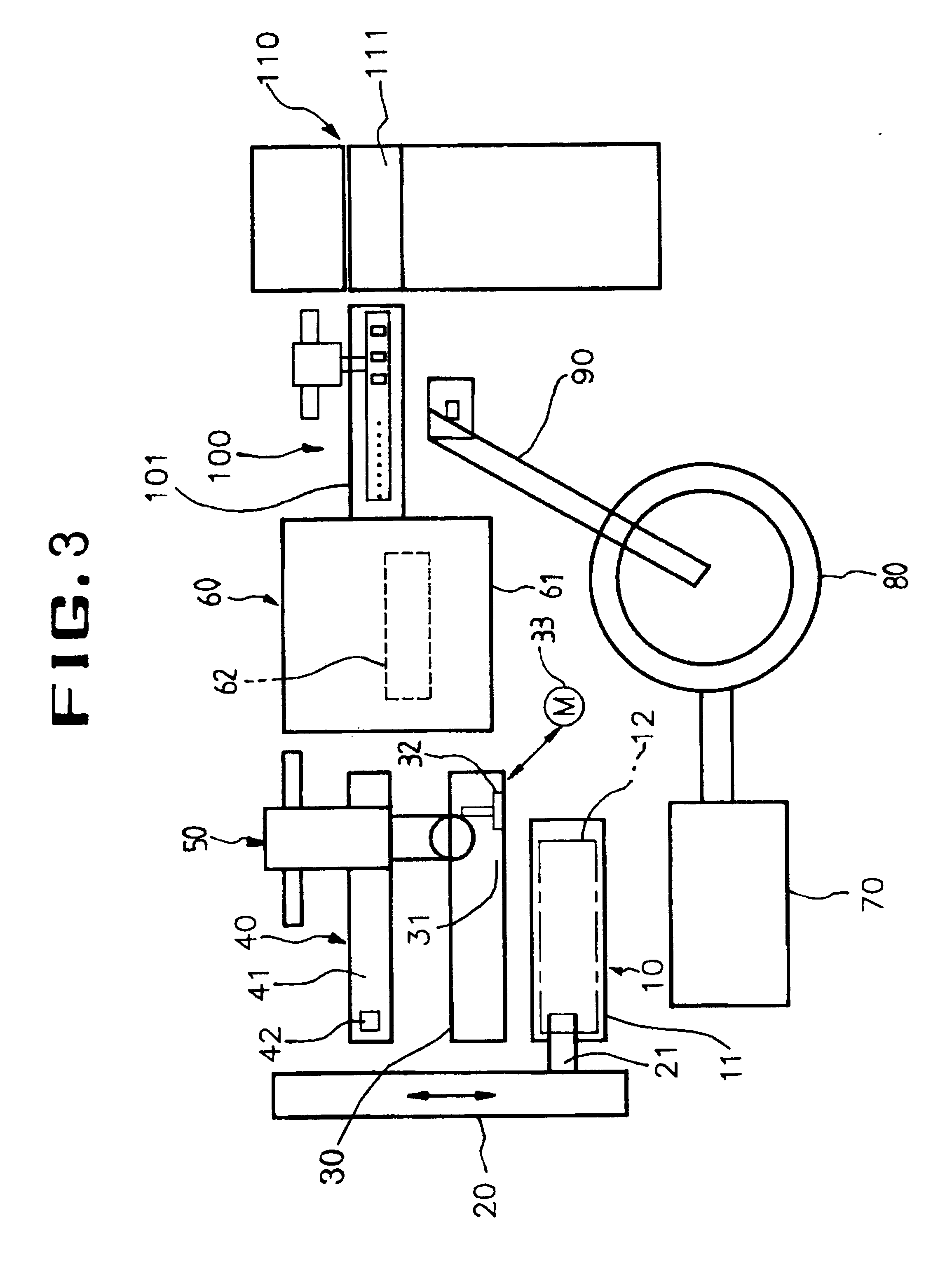
As shown in FIG. 3, the die bonding apparatus according to one embodiment of this invention includes: a lead frame supply station 10 made in the form of a loading box 11 for accommodating a plurality of lead frames 12 by way of putting one upon another; a frame transferring device 20 for picking up the lead frame 12 piled in the lead frame supply station 10 using a vacuum suction 21 and transferring it to an Ag epoxy application table 31 and then transferring it to a traveling rail 41; a frame fixing station 30 for fixing the lead frame 12, which has been transferred by the vacuum suction 21 in the frame transferring device 20, to the Ag epoxy application table 31 by adsorbing the lead frame 12 using the vacuum pump 32 or moving it b...


PUM

PropertyMeasurementUnit
Poweraaaaaaaaaa

Abstract

A die bonding apparatus includes: a lead frame supply station for accommodating a plurality of lead frames; a frame transferring device for picking up the lead frame and transferring it to an Ag epoxy application table or to a traveling rail; a frame fixing station for fixing the lead frame to the Ag epoxy application table by suction power of a vacuum pump or moving it back and forth through actuation of a motor; an Ag epoxy supply station for ejecting a predetermined amount of Ag epoxy through a nozzle to the top surface of the lead frame; a moving device for moving the lead frame forward on the traveling rail; a preheating station for receiving the lead frame into a magazine and preheating it; a wafer placement station for transferring wafers sequentially supplied from a wafer supply station to a predetermined location through rotation; a die transferring device for picking up a die and transferring it to a work site for die bonding; a die bonding station for precisely bonding the die to a site where a tape is stuck or Ag epoxy is applied in the lead frame according to lead on chip (LOC) or normal feature of the lead frame; and a stocker for accommodating the lead frame into an internal magazine.

Description

1. Field of the InventionThe present invention relates to a die bonding apparatus and, more particularly, to a die bonding apparatus for selectively performing LOC (lead on chip) die bonding and normal die bonding through regulation of a simple control function when bonding semiconductor chips of a memory device from a wafer to lead frames, thereby to increase efficiency in use of equipment and reduce the cost for equipment.2. Discussion of Related ArtA semiconductor lead frame is one of the core elements constructing a semiconductor package together with a wafer.It has been well known that the lead frame serves as both a lead for connecting the inside of the semiconductor package and the outside, or the circuit board, and a frame for supporting a semiconductor chip.This semiconductor lead frame is made in such a manner of forming a predetermined shape out of thin film material using a press dies sequentially transferred or through an etching step utilizing chemicals.The semiconduct...

Claims


Application Information

Patent Timeline
IPC IPC(8): B23K20/02H01L21/00H01L21/52H01L21/50
CPCB23K20/023H01L21/67144H01L24/743Y10T156/1749H01L2224/4826H01L2924/01078H01L2924/01079H01L2224/32245H01L2224/73215B23K2201/40Y10T156/1798Y10T428/24165Y10T156/1744Y10T428/24231Y10T156/1768H01L2924/10253H01L2224/743H01L2924/00H01L2224/83048B23K2101/40H01L2224/48091H01L2224/73265H01L2924/00014H01L21/52
Inventor KIM, SEONG-BONGYEOM, MYEONG-KYU
Owner SAMSUNG ELECTRONICS CO LTD
Why Eureka
Try Eureka