Organic pin grid array flip chip carrier package

a chip carrier and flip chip technology, applied in the field of organic carrier components, can solve the problems of high cost, high cost, and small size of devices, and achieve the effect of avoiding the possibility of high soldering temperature and high cos

Inactive Publication Date: 2001-05-08
ADVANCED MICRO DEVICES INC
View PDF20 Cites 33 Cited by
  • Summary
  • Abstract
  • Description
  • Claims
  • Application Information

AI Technical Summary

Problems solved by technology

The escalating requirements for high density and performance associated with ultra-large scale integration technology creates significant challenges for the design and implementation of electrical connections between circuit components and external electrical circuitly.
These devices are typically very small and fragile.
One problem associated with attaching pin leads to metallized pads o...

Method used


Image

  • Organic pin grid array flip chip carrier package
  • Organic pin grid array flip chip carrier package
  • Organic pin grid array flip chip carrier package

Examples


Embodiment Construction

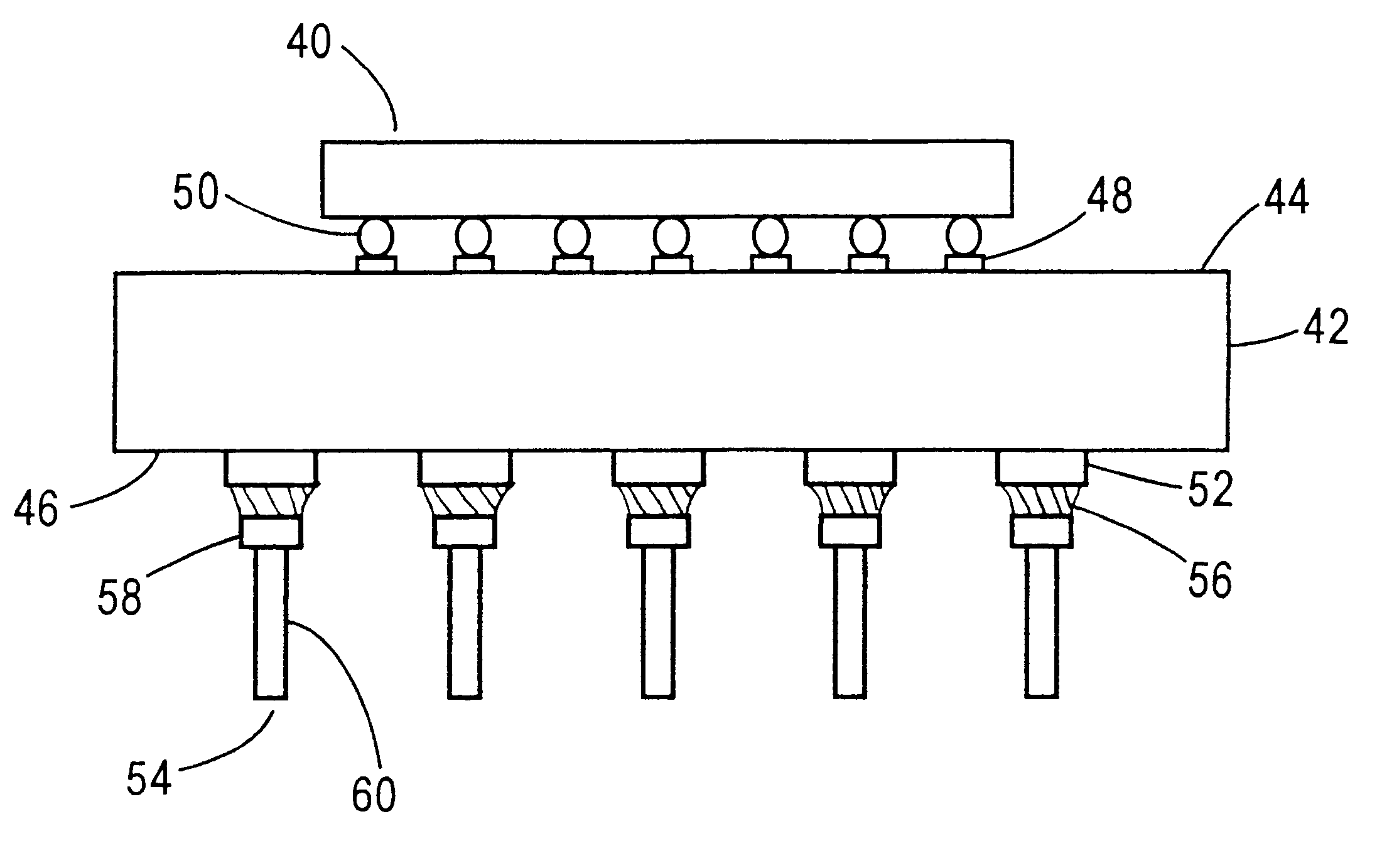
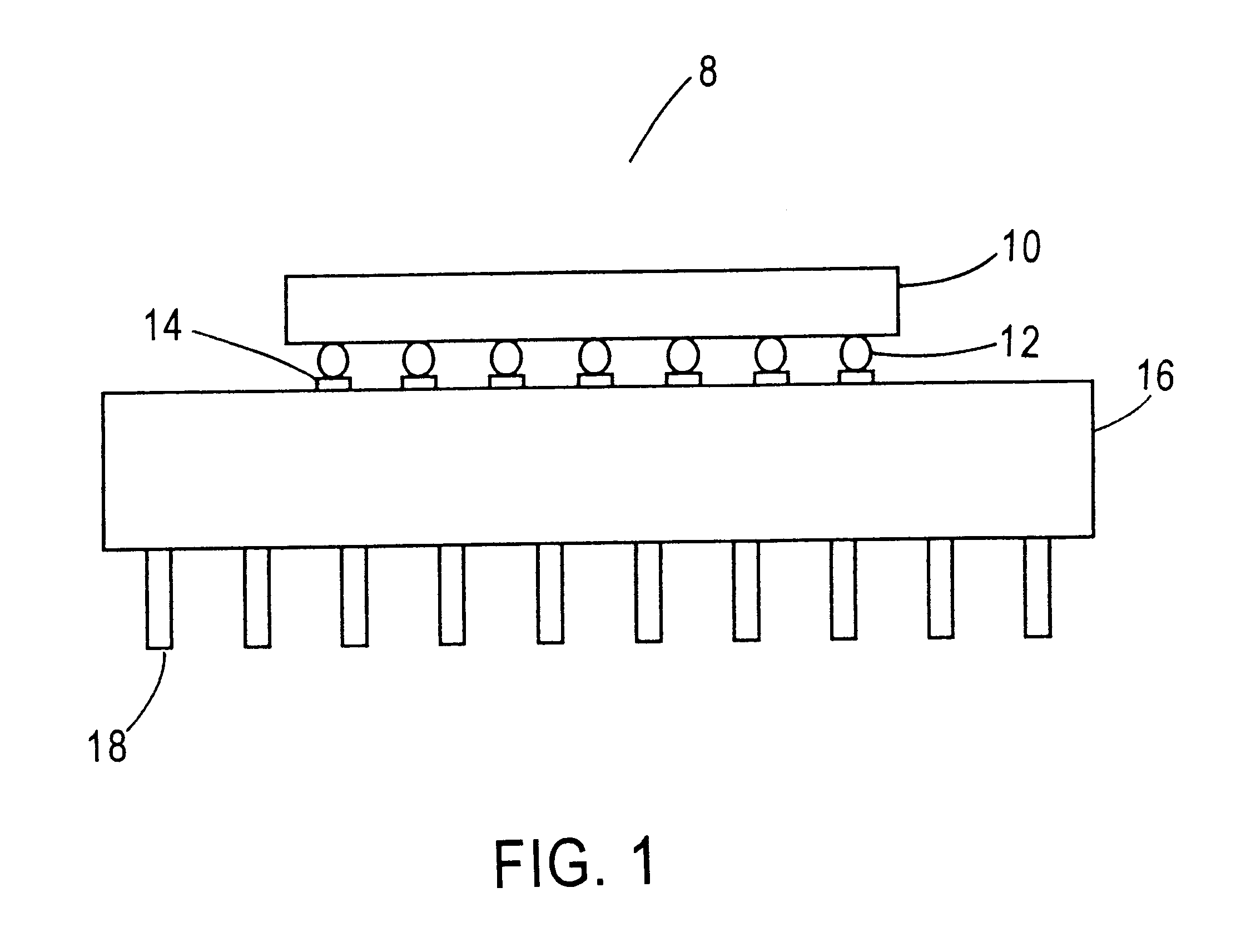
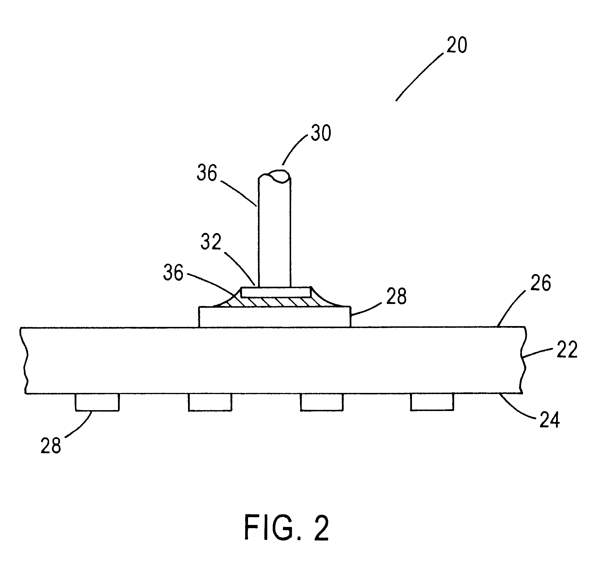
The present invention stems from the discovery that employing solder fillets having a high reflow temperature and low tin content to mechanically and electrically bond a pin lead to a conductive pad on an organic substrate reduces or eliminates several problems associated with attaching pin leads to organic packages. In particular, it was discovered that solder fillets having a low tin content can be prepared that reflow below the decomposition temperature of the organic substrate yet strongly joins pin leads to conductive pads with little or no solder climbing up the pin shaft.

In order to address the difficulty of providing a highly reliable organic pin grid array carrier member, it was necessary to gain an understanding of the causes of the problems associated with attaching pin leads to the member. One problem that conventional, high tin solders encounter in bonding I / O pins to organic carrier members is that the conventional solders partially melt in subsequent thermal processin...


PUM


Abstract

An organic carrier member for mounting a semiconductor device is provided that has a plurality of pin leads joined to conductive pads on the carrier member by a solder fillet having a reflow temperature higher than the temperature necessary to attach the semiconductor device. Embodiments include a bismaleimide-triazine epoxy laminate carrier member having an array of pins joined to the carrier member by a solder fillet having a reflow temperature of no greater than 275° C.

Description

1. Field of the InventionThe present invention relates to an organic carrier member for mounting a semiconductor device, and more particularly to an organic carrier member having pin leads mounted thereon.2. Background ArtThe escalating requirements for high density and performance associated with ultra-large scale integration technology creates significant challenges for the design and implementation of electrical connections between circuit components and external electrical circuitly.Integrated circuit (IC) devices whether individual active devices, individual passive devices, multiple active devices within a single chip, or multiple passive and active devices within a single chip, require suitable input / output (I / O) connections between themselves and other circuit elements or structures. These devices are typically very small and fragile. Because of their size and fragility, they are commonly carried on substrates for support, i.e., carrier members.Device miniaturization and the...

Claims


Application Information

Patent Timeline
IPC IPC(8): H01L23/498H01L23/48H05K3/34
CPCH01L23/49811H05K3/3463H01L2224/16225H01L2924/01079H01L2924/15312H01L2924/01087H01L2924/01322
Inventor MASTER, RAJ N.
Owner ADVANCED MICRO DEVICES INC
Why Eureka
Try Eureka