A/D converter
- Summary
- Abstract
- Description
- Claims
- Application Information
AI Technical Summary
Problems solved by technology
Method used
Image
Examples
first embodiment
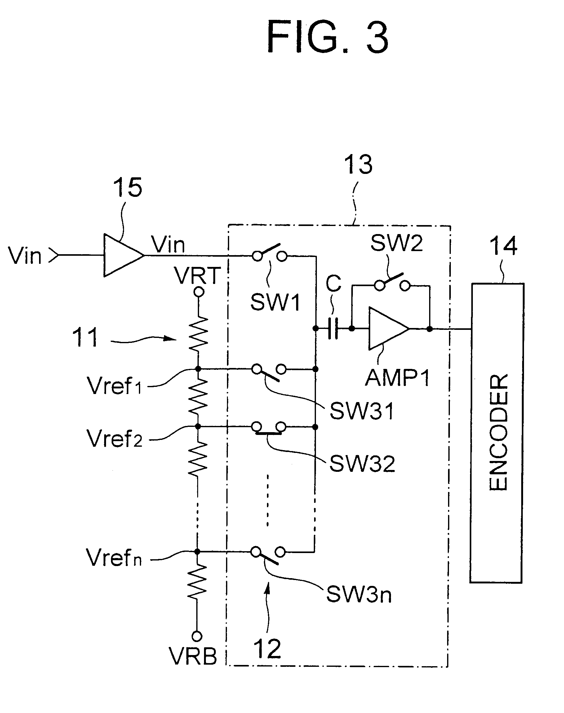
An A / D converter of the present invention shown in FIG. 3 includes an input buffer 15 to which an analogue signal Vin is input, a resistor ladder 11 for outputting reference voltages Vref1 to Vrefn (n=2.sup.N -1) connected between a first reference source line VRT and a second reference source line VRB, a comparator 13 for comparing the respective reference voltages Vref1 to Vrefn from the resistor ladder 11 with the analogue signal Vin input from the input buffer 15, and an encoder 14 for sequentially encoding output signals from the comparator 13.
The comparator 13 has a first switch SW1 having a first terminal connected to the output of the input buffer 15, an array of switches 12 including "n" second switches SW31 to SW3n each having a first terminal connected to each of the corresponding reference voltage output nodes Vref1 to Vrefn and a second terminal connected in common to a second terminal of the first switch SW1, a charge capacitor C having a first terminal connected to th...
second embodiment
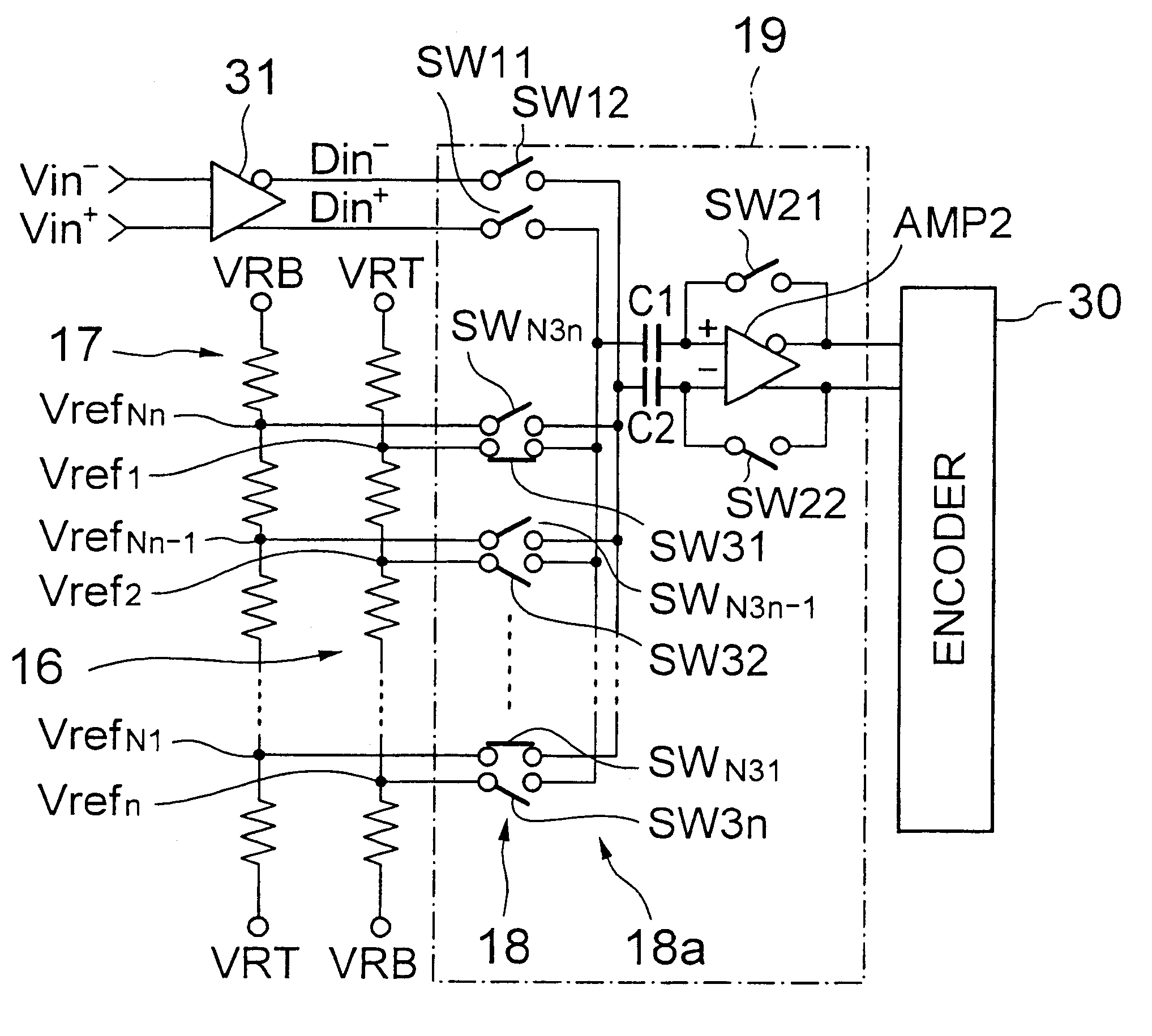
the present invention is illustrated in FIG. 4 in which two resistor ladders 16 and 17 are shown for avoiding complication of the drawing. However, these two ladders may be combined into one ladder. An A / D converter of this embodiment is an example of converting an analogue differential input signals Vin- and Vin+ into digital signals.
An input differential amplifier 31 receives differential input signals Vin+ and Vin- and outputs a non-inverted signal Din+ and an inverted signal Din- of differential outputs of the input signals to transfer the signals to a comparator 19. The first ladder 16 and the second ladder 17 are connected in parallel between a first reference source line VRT and a second reference source line VRB. The first ladder 16 outputs "n" reference voltages in a range from a maximum reference voltage Vref1 to a minimum reference voltage Vrefn, and the second ladder 17 outputs "n" reference voltages in a range from a minimum reference voltage VrefN1 to a maximum referen...
PUM
 Abstract
Description
Claims
Application Information
 - R&D Engineer
- R&D Manager
- IP Professional
- Industry Leading Data Capabilities
- Powerful AI technology
- Patent DNA Extraction
Browse by: Latest US Patents, China's latest patents, Technical Efficacy Thesaurus, Application Domain, Technology Topic, Popular Technical Reports.
© 2024 PatSnap. All rights reserved.Legal|Privacy policy|Modern Slavery Act Transparency Statement|Sitemap|About US| Contact US: help@patsnap.com


