Printed circuit board for coupling surface mounted optoelectric semiconductor devices

a technology of optoelectronic devices and printed circuit boards, which is applied in the association of printed circuit non-printed electric components, electric apparatus casings/cabinets/drawers, instruments, etc., and can solve problems such as electronic components

Inactive Publication Date: 2001-05-08
IBM CORP
View PDF20 Cites 86 Cited by
  • Summary
  • Abstract
  • Description
  • Claims
  • Application Information

AI Technical Summary

Problems solved by technology

Thus, both the limitations in materials and the limitations in electronic co

Method used


Image

  • Printed circuit board for coupling surface mounted optoelectric semiconductor devices
  • Printed circuit board for coupling surface mounted optoelectric semiconductor devices
  • Printed circuit board for coupling surface mounted optoelectric semiconductor devices

Examples


Embodiment Construction

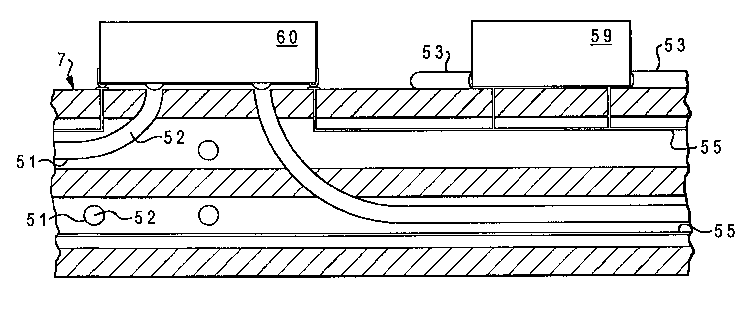
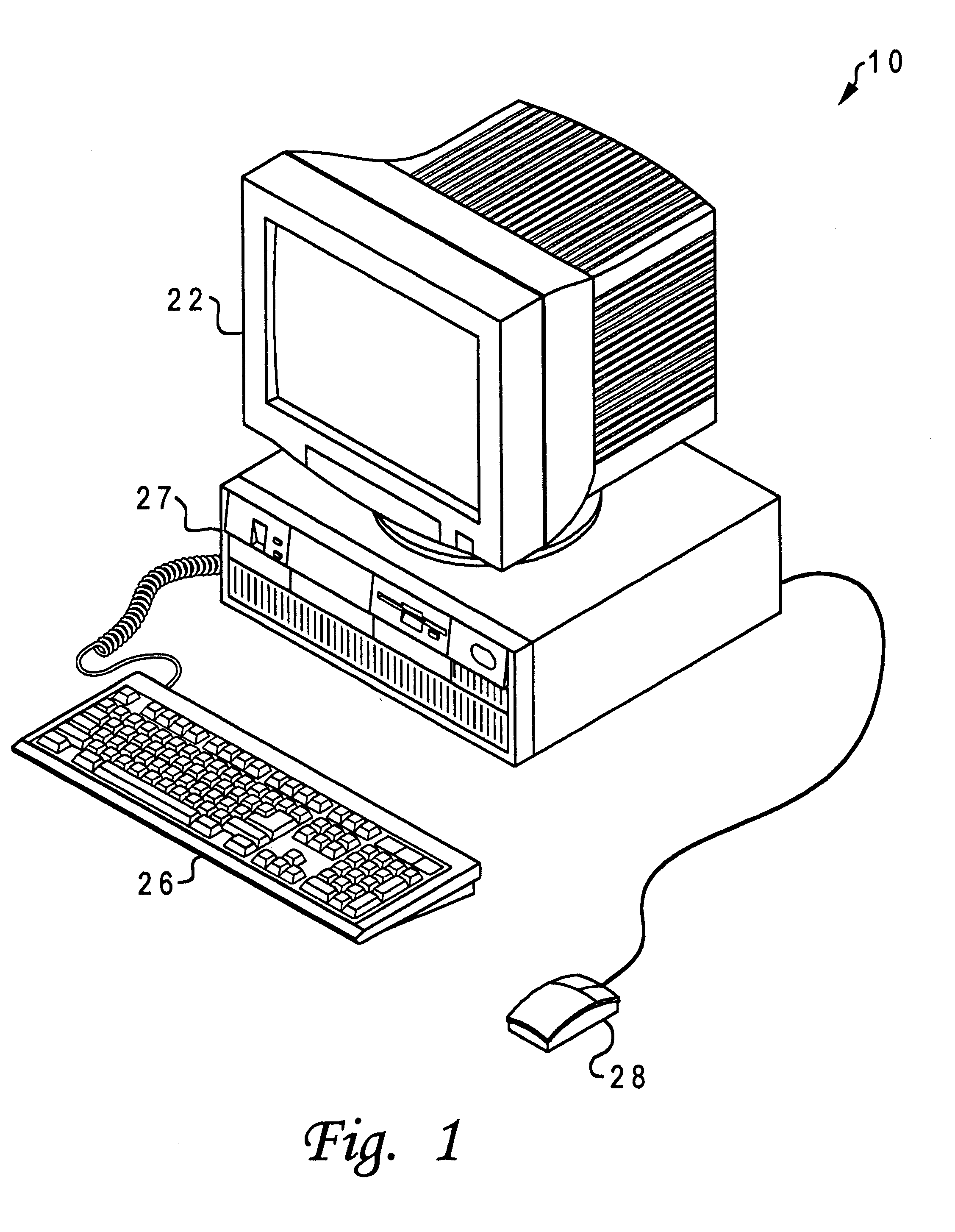
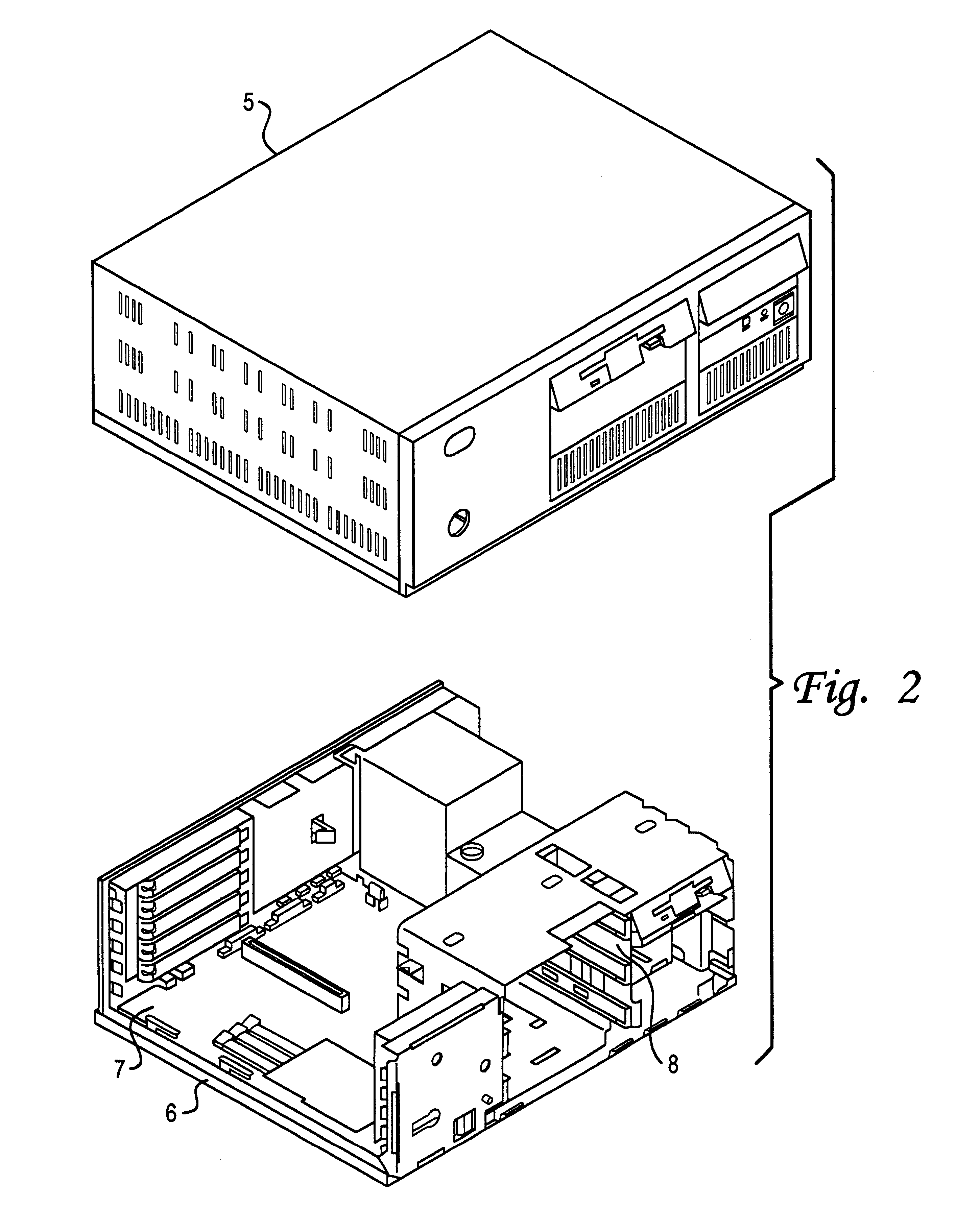
Referring now to the drawings and in particular to FIG. 1, there is depicted a block diagram of an optoelectric computer system to which a preferred embodiment of the present invention is applicable. An optoelectric computer system 10 includes a computer unit 27, a monitor 22, a keyboard 26, and a mouse 28. As shown in FIG. 2, computer unit 27 has a cover 5 that cooperates with a chassis 6 in defining an enclosed, shielded volume for receiving electrically powered data processing components. Some of the data processing components are mounted on a printed circuit board (or motherboard) 7 that is secured within chassis 6. Chassis 6 has a base and a rear panel and defines at least one open bay for receiving a data storage device such as a magnetic disk drive, an optical disk drive, or the like. As shown, an upper bay 8 is adapted to receive a floppy disk drive (not shown).

Referring now to FIG. 3, there is illustrated a block diagram of 17 various components within optoelectric computer...


PUM


Abstract

A printed circuit board for coupling surface mounted optoelectric semiconductor devices within a computer system is disclosed. The printed circuit board includes at least one substantially planar surface. There are multiple electrically conductive sites located on the substantially planar surface for connection to a surface mounted semiconductor electronic device. The electrically conductive sites are also connected to electrical interconnects embedded within the printed circuit board. In addition, there are multiple optical pathways terminated at the substantially planar surface for coupling a surface mounted semiconductor optoelectric device.

Description

1. Technical FieldThe present invention relates to printed circuit boards in general, and in particular to a printed circuit board to be utilized in an optoelectric data processing system. Still more particularly, the present invention relates to a printed circuit board for coupling surface mounted semiconductor optoelectric devices within an optoelectric computer system.2. Description of the Prior ArtWithin most computer systems, a bus (or a group of buses) is typically the primary vehicle by which communication among electronic components takes place. Although there are different types of buses, in its most basic form, each bus is simply a series of electrical wires interconnecting various electronic components within a computer system. The electrical transmission characteristics of a bus are defined by the material properties of the bus, the physical geometry of the components, the clock speed of the signals, and the noise within the bus. Thus, both the limitations in materials a...

Claims


Application Information

Patent Timeline
IPC IPC(8): H05K9/00H05K1/02G02B6/42G02B6/43
CPCG02B6/43H05K9/0039G02B6/4246H05K1/0274
Inventor MUNOZ-BUSTAMANTE, CARLOSMCCONNELL, DANIEL
Owner IBM CORP
Why Eureka
Try Eureka