

Linear ramping digital-to-analog converter for integrated circuit tester
a digital-to-analog converter and integrated circuit technology, applied in the field of linear ramping digital-to-analog converters, can solve the problems of high cost of high-frequency dacs, limited flexibility of waveform generators in producing outputs, and inability to set square waves
- Summary
- Abstract
- Description
- Claims
- Application Information
AI Technical Summary
Benefits of technology
Problems solved by technology
Method used
Image

Examples
Embodiment Construction
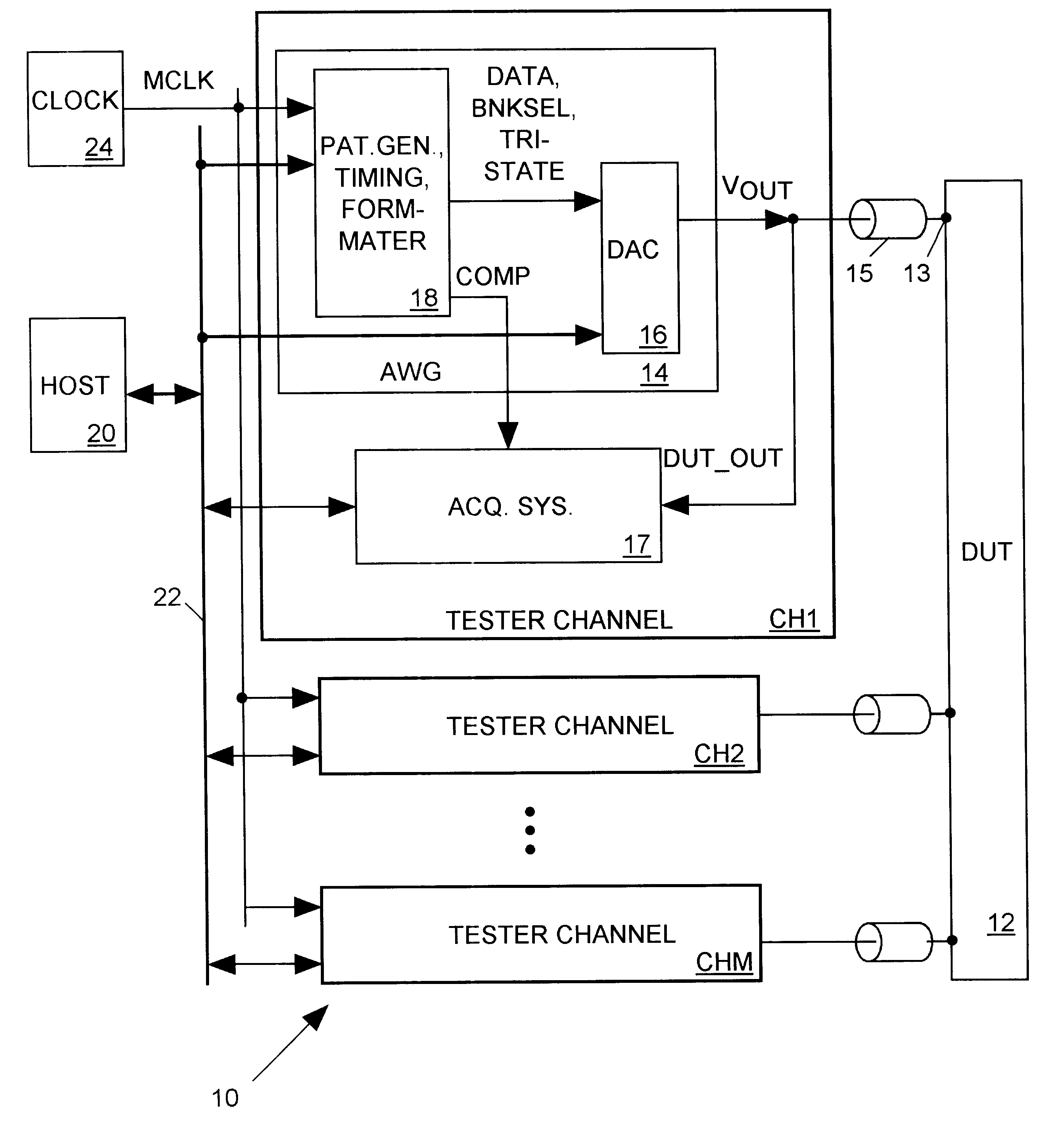
IC Tester Architecture
A typical high speed digital integrated circuit (IC) tester tests the logic of an IC by applying square wave test signals to IC input terminals. The present invention relates to an improved IC tester that can provide not only square wave signals but signals of arbitrary waveform shapes as inputs to an IC. For example in order to test an IC's ability to tolerate noise a tester in accordance with the present invention may produce a square wave test signal upon which it has superimposed an oscillating signal component simulating various noise levels and frequencies. Or, as another example, the IC tester of the present invention can be used to test analog ICs by producing test signals simulating sine wave or other smoothly varying signals.
FIG. 1 illustrates an integrated circuit (IC) tester 10 in accordance with the invention for testing an IC device under test (DUT) 12. Tester 10 includes a set of channels CH1-CHM, each capable of generating and transmitting a tes...
PUM
 Abstract
Description
Claims
Application Information