High-frequency oscillator using FETs and transmission lines

a transmission line and high-frequency oscillator technology, applied in the direction of oscillator generators, pulse techniques, semiconductor/solid-state device details, etc., can solve the problems of difficult control of 1/f noise, 1/f noise, phase error tends to occur between the input and output of the

Inactive Publication Date: 2001-05-29
NEC ELECTRONICS CORP
View PDF7 Cites 34 Cited by
  • Summary
  • Abstract
  • Description
  • Claims
  • Application Information

AI Technical Summary

Problems solved by technology

In a high-frequency oscillator using an FET where the output of the FET is positively fedback to its input, generally, some phase error tends to occur between the input and output of the FET due to the 1 / f noise and the white noise generated in the FET.
The main cause of the 1 / f noise is the time constant distribution of the recombination centers existing at the surfaces of the semiconductor of the FET and the interfaces therein.
Therefore, not only the 1 / f noise is difficult to be controlled but also it tends to affect the lateral-type semiconductor device such as the FET.
However, it has a problem that the mass productivity is not high and that the oscillator size or scale is large.
This is due to the fact that the 1 / f noise was not considered in the simulation.
As a result, it is found that from the view point of usefulness, the phase noise of the prior-art oscillator of FIG. 3 is not satisfactorily low for the use in the high frequency range of 60 GHz or higher.
As explained above, the prior-art oscillator shown in FIG. 2 has the problem that the mass productivity is not high and the oscillator size or scale is large.
The prior-art oscillator shown in FIG. 3 has the problem that the phase noise is high.

Method used


Image

  • High-frequency oscillator using FETs and transmission lines
  • High-frequency oscillator using FETs and transmission lines
  • High-frequency oscillator using FETs and transmission lines

Examples


first embodiment

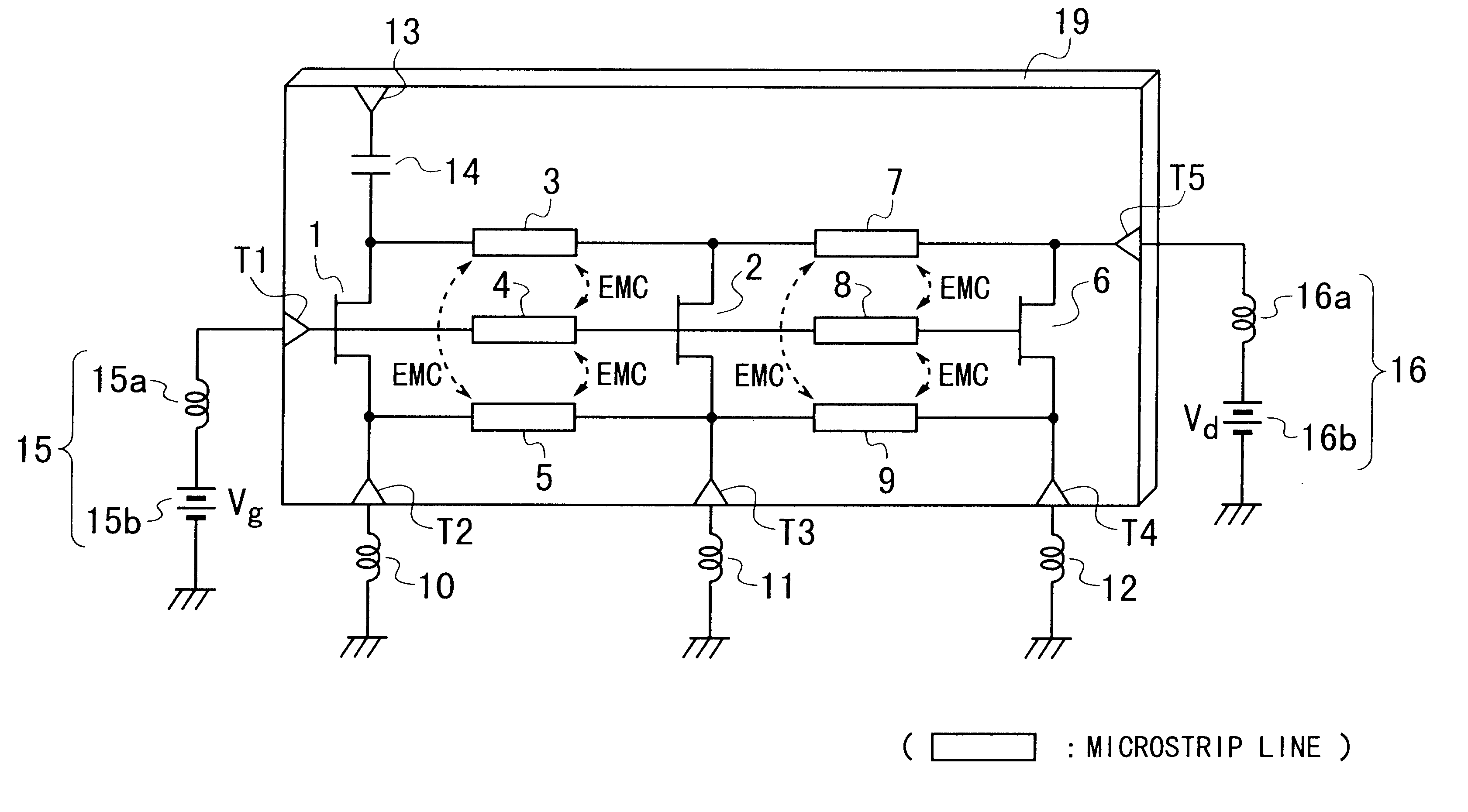
A high-frequency oscillator according to the invention has the circuit configuration as shown in FIG. 7.

As seen from FIG. 7, the oscillator comprises three FETs 1, 2, and 6 and six transmission lines 3, 4, 5, 7, 8, and 9, which are formed on a GaAs substrate 19. Each of the lines 3, 4, 5, 7, 8, and 9 is formed by a microstrip line. The lines 3, 4, and 5 are arranged in parallel on the substrate 19 and electromagnetically coupled with each other. In other words, the lines 3, 4, and 5 are coupled together due to the electromagnetic field. Similarly, the lines 7, 8, and 9 are arranged in parallel on the substrate 19 and electromagnetically coupled with each other. In other words, the lines 7, 8, and 9 are coupled together due to the electromagnetic field.

The gate of the first FET 1 is connected to a corresponding end of the transmission line 4. The gate of the first FET 1 is further connected to one terminal of a gate bias circuit 15 through an interconnection terminal T1. The other te...

second embodiment

FIG. 10 shows a high-frequency oscillator according to a second embodiment of the invention, which has the same configuration as that of the first embodiment except that transmission lines 26, 27, and 28 are used instead of the inductors 10, 11, and 12 in the first embodiment. Accordingly, the explanation about the same configuration is omitted here for simplification of description by attaching the same reference symbols as those used in the first embodiment in FIG. 10.

As shown in FIG. 10, the transmission lines 26, 27, and 28 are microstrip lines formed on the GaAs substrate 19. The line 26 is connected to the source of the first FET 1 and the interconnection terminal T2. The line 27 is connected to the source of the second FET 2 and the interconnection terminal T3. The line 28 is connected to the source of the third FET 6 and the interconnection terminal T4.

To examine the performance of the oscillator according to the second embodiment of FIG. 10, the inventor carried out simulat...

third embodiment

FIG. 13 shows a high-frequency oscillator according to a third embodiment of the invention, which has the same configuration as that of the second embodiment except that an alumina (Al.sub.2 O.sub.3) substrate 39 is used instead of the GaAs substrate 19 in the first embodiment. Accordingly, the explanation about the same configuration is omitted here for simplification of description by attaching the same reference symbols as those used in the second embodiment in FIG. 13.

As seen from FIG. 13, because of the substrate 39 is dielectric, the first to third FETs 1, 2, and 6 are formed by discrete transistors 31, 32, and 33, respectively. The capacitor 14 also is formed by a discrete capacitor component 34. The transistors 31, 32, and 33, and the capacitor component 34 are mounted on the substrate 39 by the well-known flip-chip bonding technique.

To examine the performance of the oscillator according to the third embodiment of FIG. 13, the inventor carried out simulation in the same mann...


PUM


Abstract

A high-frequency oscillator is provided, which decreases the phase noise and which has excellent mass productivity and reproducibility. This oscillator is comprised of (a) first, second, and third FETs formed on a substrate; (b) a first transmission line formed on the substrate; the first line being connected to drains of the first and second FETs formed on the substrate; (c) a second transmission line formed on the substrate; the second line being connected to gates of the first and second FETs; (d) a third transmission line formed on the substrate; the third line being connected to sources of the first and second FETs; (e) a fourth transmission line formed on the substrate; the fourth line being connected to the drain of the second FET and a drain of the third FET; (f) a fifth transmission line formed on the substrate; the fifth line being connected to the gate of the second FET and a gate of the third FET; and (g) a sixth transmission line formed on the substrate; the sixth line being connected to the source of the second FET and a source of the third FET. The first, second, and third transmission lines are coupled together due to electromagnetic field, and the fourth, fifth, and sixth transmission lines are coupled together due to electromagnetic field.

Description

1. Field of the InventionThe present invention relates to a high-frequency oscillator. More particularly, the invention relates to a high-frequency oscillator using Field-Effect Transistors (FETs) and electromagnetically-coupled transmission lines, which is applicable to the microwave or millimeter wave ranges.2. Description of the Prior ArtIn a high-frequency oscillator using an FET where the output of the FET is positively fedback to its input, generally, some phase error tends to occur between the input and output of the FET due to the 1 / f noise and the white noise generated in the FET. The resonant or oscillation frequency of the oscillator shifts automatically so as to eliminate or decrease the phase error according to the Kirchhoff's law. Thus, the oscillation frequency tends to fluctuate, resulting in a wide-based spectrum B in FIG. 1.Ideally, the oscillation frequency of the oscillator is kept at a single value and therefore, it has a linear spectrum A shown in FIG. 1, i.e.,...

Claims


Application Information

Patent Timeline
Patent Type & Authority Patents(United States)
IPC IPC(8): H03B5/18
CPCH03B5/1847
Inventor MIZUTANI, HIROSHI
Owner NEC ELECTRONICS CORP
Why Eureka
Try Eureka