Circuit trace probe and method

a circuit trace and probe technology, applied in the field of circuit trace probes, can solve the problems of affecting the accuracy and completeness of the test, and not always being possible to do

Inactive Publication Date: 2001-06-05
GLOBALFOUNDRIES INC
View PDF9 Cites 11 Cited by
  • Summary
  • Abstract
  • Description
  • Claims
  • Application Information

AI Technical Summary

Problems solved by technology

Obviously, the testing and validation process used to test the electrical circuits and the printed circuit boards is not error-free.
Unfortunately, while the theory of product testing is sound, the actual testing of circuit and PCBs is often subject to real world constraints that may hinder accurate and complete testing results.
While it may be desirable to add multiple test points on a PCB to facilitate production testing, it will not always be possible to do so.
Each electrical contact point occupies precious space and may impede board functionality.
Thus, testability may be lost in a tradeoff with functionality.
In addition, the product design engineers responsible for designing the circuits and PCBs are typically not the individuals responsible for testing the circuits and PCBs.
The design engineers may not place a high emphasis on production testability and, therefore, may not incorporate sufficient test points.
The addition of new test points after initial design has been completed may require the design engineers to repeat considerable work, thereby increasing costs and delaying product introduction.
Also, once a circuit or PCB design has been approved by management, design changes to include additional desirable test points may, as a practical matter, no longer be feasible.
These practical realities are somewhat disconcerting to a production test engineer who is given the responsibility to ensure quality control for shipping products.
However, due to the practical constraints explained above, this is typically very difficult to accomplish, if not impossible.
Without new methods or techniques to allow additional test points to be created on a given PCB, the electronics industry will continue to be limited in the ability to improve the reliability of newly designed and manufactured products.
If the circuits on a chip contain a flaw, an incorrect logic function may result.
As within the individual components, if the traces between the components are flawed, an incorrect logic function for the PCB as a whole may result.
In this way, defects in board fabrication may be identified.
If the board fails to function properly, the reason for the failure may very difficult to find due to the inherently limited diagnostic capability of a functional test.
In addition, given the practical testing limitations outlined above, ascertaining the reason for board failure may be impossible, and is almost always time consuming and expensive.
However, as explained above, in-circuit testing requires sufficient test points to perform thorough testing and is subject to various real-life constraints that may or may not facilitate effective testing of the printed circuit board's functionality.

Method used


Image

  • Circuit trace probe and method
  • Circuit trace probe and method
  • Circuit trace probe and method

Examples


Embodiment Construction

Creating Test Points

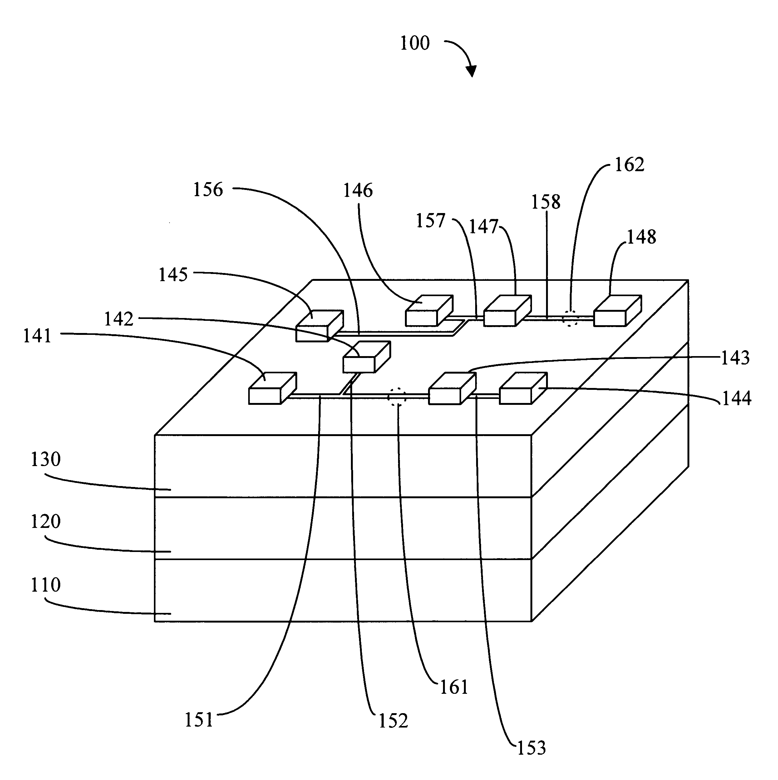
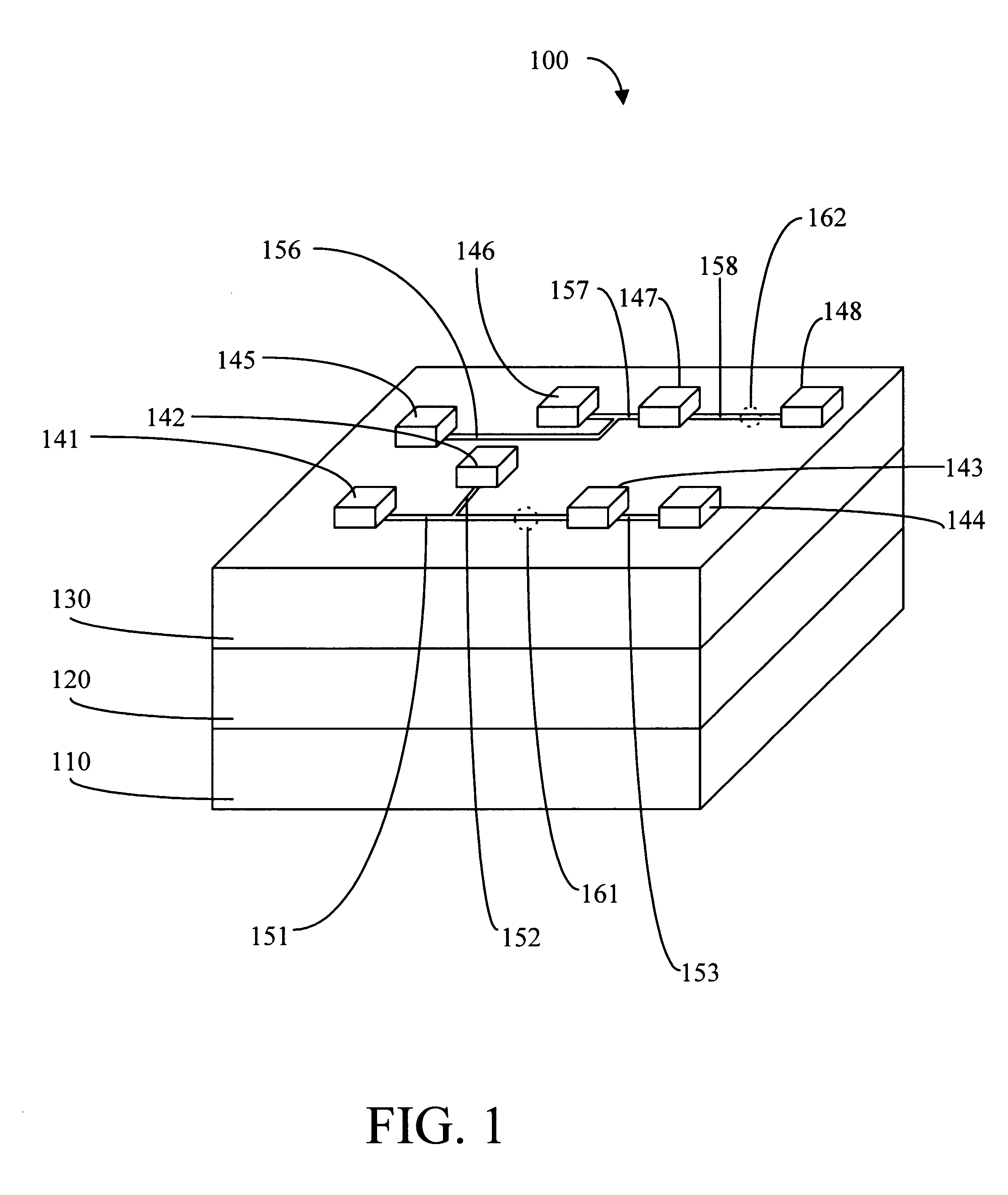
The present invention overcomes the obstacle of having too few traditional test points on a designed board by establishing openings or access points in the procoat to allow circuit traces or points on the circuit traces to be used as new, additional test points for testing PCBs. In addition, the present invention teaches the use of a specially designed test probe to contact the new test points. The invention may be used after the functional design of a circuit board has been completed but before large scale fabrication has begun and may also be used for reliability testing and / or troubleshooting of finished printed circuit boards.

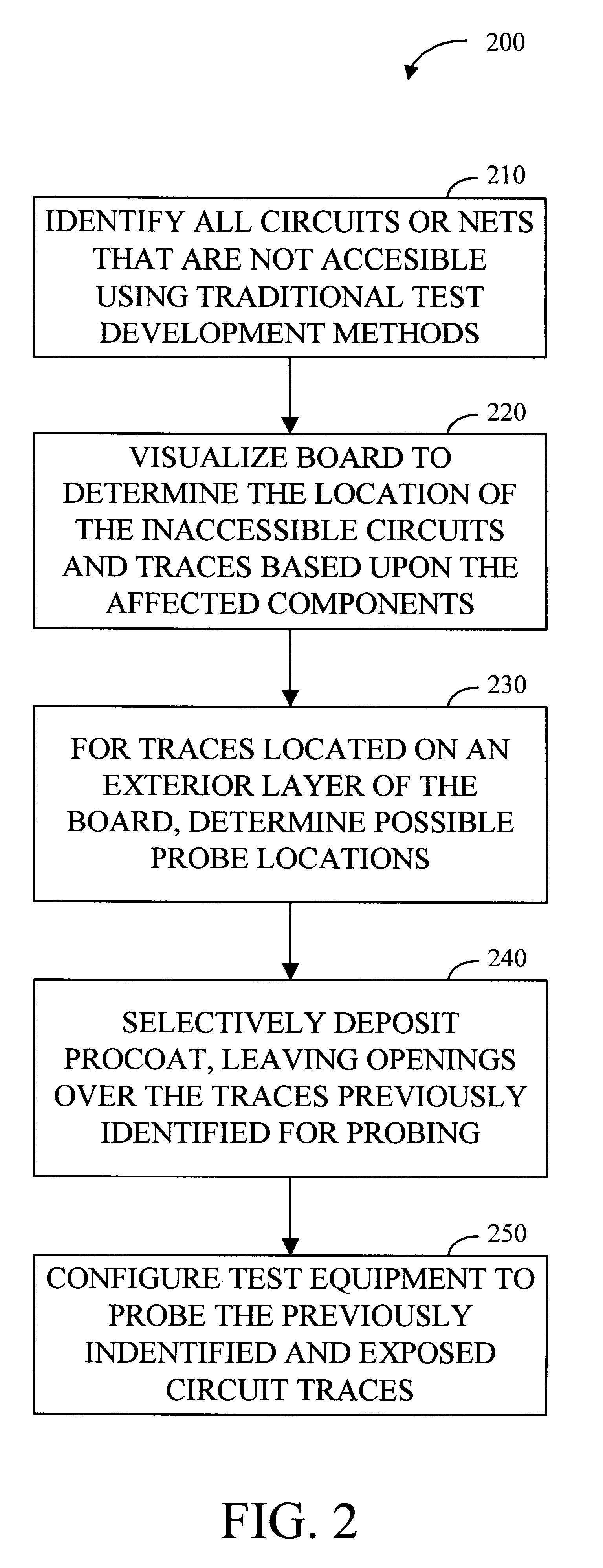
Referring now to FIG. 2, a method 200 for creating new test points is explained. First, the test engineer identifies or determines which circuits or nets on a PCB are untestable using the traditional testing procedures and test points which were established during the design phase for the PCB (step 210). The engineer will also note which...


PUM


Abstract

According to the preferred embodiments of the present invention, a method of creating and accessing additional test points after circuit board design has been completed is disclosed. The apparatus and methods of the present invention provide test engineers with the ability to leave any circuit interconnections located on the exterior surfaces of a PCB exposed. These exposed circuit interconnections may be identified as access or test points and the apparatus of the present invention is specifically adapted to access, probe, and evaluate these access or test points. To allow the exposed circuit interconnections to be tested without damaging them, the invention includes a new type of probe for use in contacting the exposed traces. The preferred embodiments of the test probe apparatus of the present invention has a relatively flat head to reduce pressure on the circuit interconnections and is coated with dendrites to enhance electrical connectivity between the circuit interconnections and the probe. By using both the apparatus and the methods of the present invention, additional test points may be created on the surface of a PCB after circuit and board design has been completed.

Description

1. Technical FieldThis invention relates generally to fabricating electrical components and more specifically relates to the testing of circuits on a printed circuit board.2. Background ArtElectronic devices have become a vital part of everyday life in this country and throughout the world. Most electronic devices contain large numbers of digital electronic components and analog circuit components that work together to perform various logical operations. The various individual components in many electronic devices are typically linked into circuits on layered printed circuit boards (PCBs). These commonplace electrical circuits control everything from computers to cars to garage door openers to satellites. As new devices are developed, the capabilities of the resulting electronic circuits and components provide increased functionality, usually at a lower cost.As with any industry, electronic and electrical products are tested prior to introduction into the marketplace. Typically, mos...

Claims


Application Information

Patent Timeline
Patent Type & Authority Patents(United States)
IPC IPC(8): G01R1/067G01R31/28H05K1/02H05K3/28
CPCG01R31/2805H05K1/0268H05K3/28G01R1/06722
Inventor CAGGIANO, RAYMOND J.COLPO, CHARLESHATLEY, JEFFREY A.SOROKA, W. PETERWATTS, RONDELL K.
Owner GLOBALFOUNDRIES INC
Why Eureka
Try Eureka