Method of fabricating a trench capacitor

Inactive Publication Date: 2001-06-26
PROMOS TECH INC
View PDF6 Cites 29 Cited by
  • Summary
  • Abstract
  • Description
  • Claims
  • Application Information

AI Technical Summary

Problems solved by technology

However, since each capacitor lie within an area cannot be larger than the size of the cell area in order to accommodate all the capacitors in the large array of cells used on the DRAM device.
It is becoming increasing

Method used


Image

  • Method of fabricating a trench capacitor
  • Method of fabricating a trench capacitor
  • Method of fabricating a trench capacitor

Examples


Embodiment Construction

A preferred embodiment of the invention is described below. This embodiment is merely exemplary. Those skilled in the art will appreciate that changes can be made to the disclosed embodiment without departing from the spirit and scope of the invention.

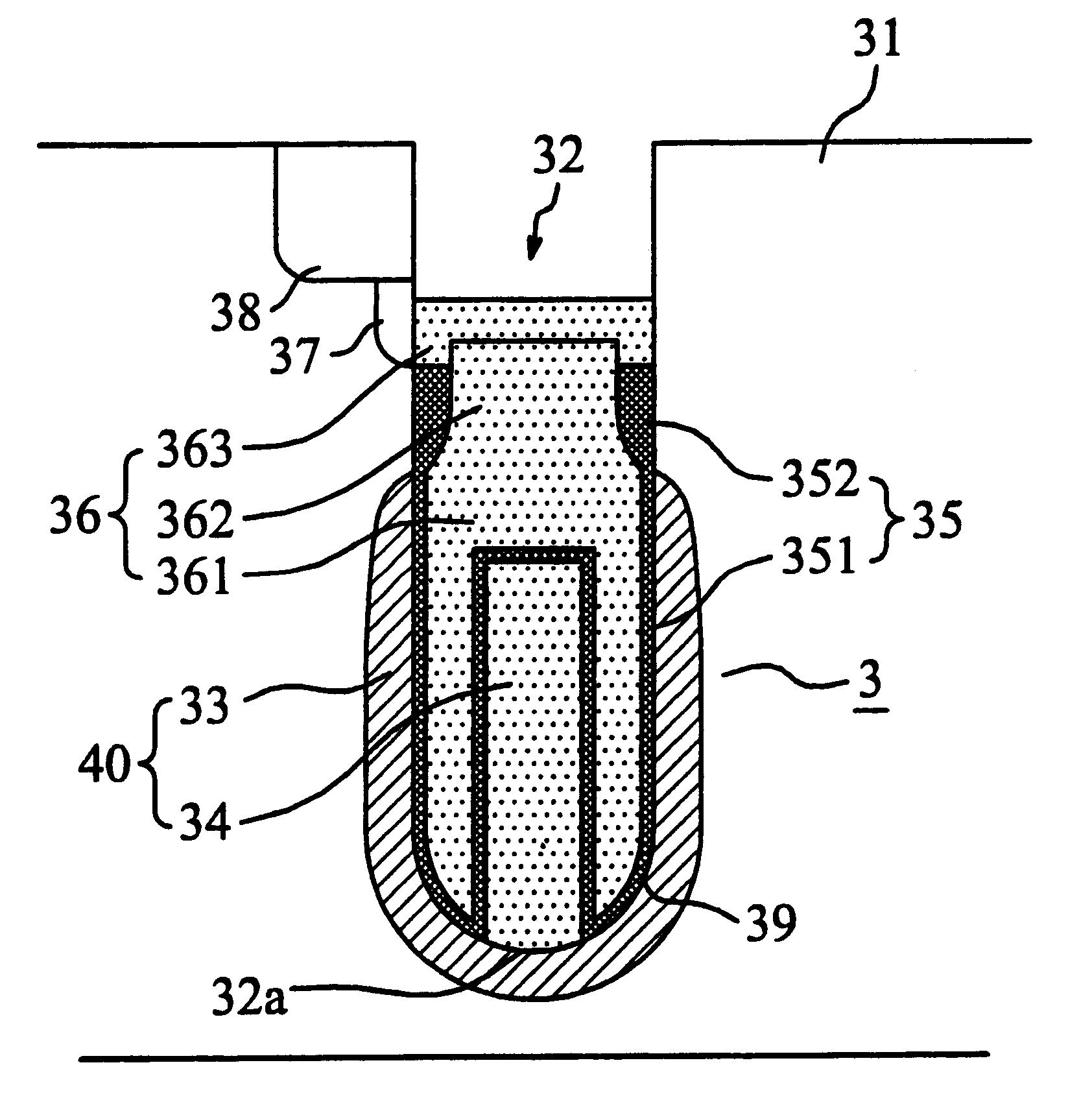
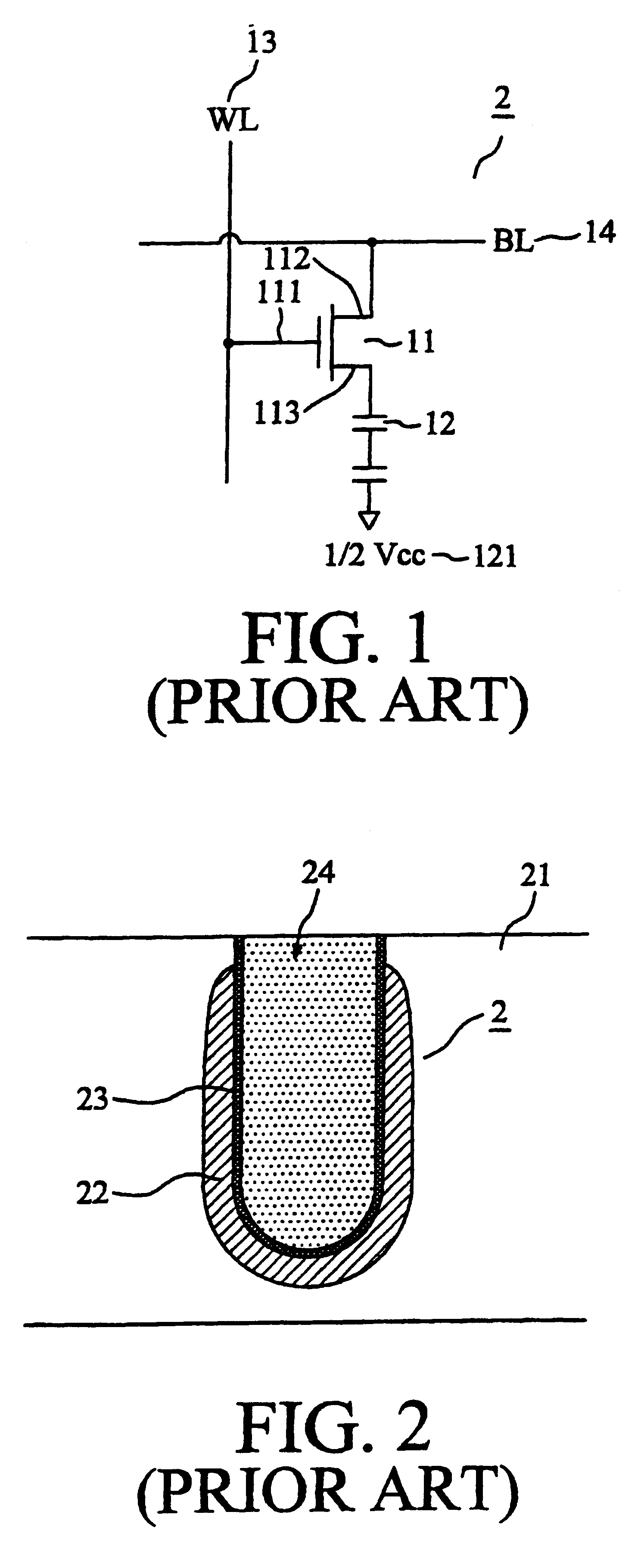
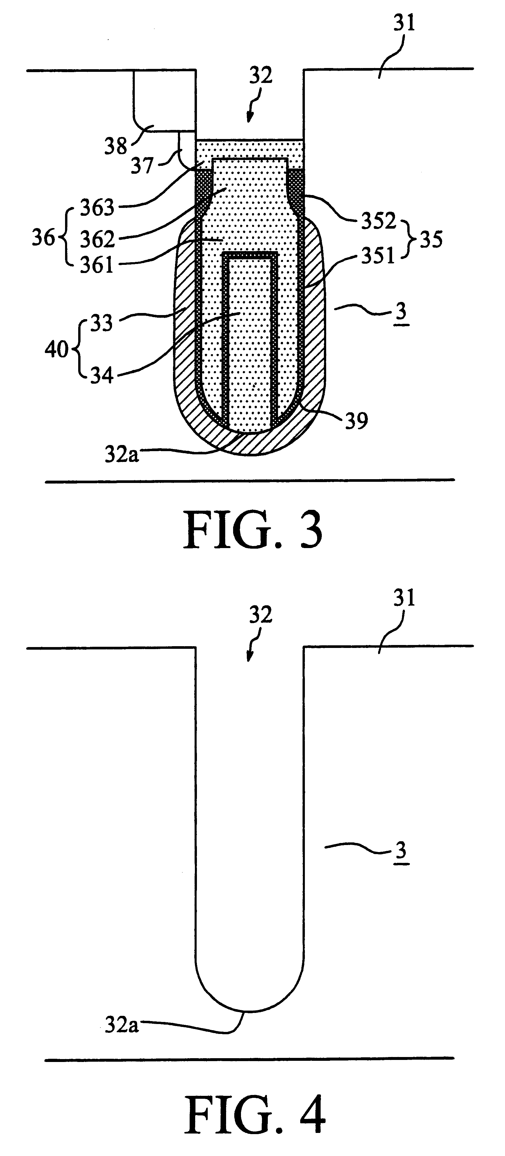
Refer to FIG. 3, the trench capacitor 3 of the present invention includes a p-type semiconductor substrate 31, a trench 32 formed on the p-type semiconductor substrate 31. The trench 32 is composed of a bottom portion 32a and at least one sidewall 39. A bottom electrode 40 is composed of an n-type impurity diffusion layer 33 and a polysilicon layer 34. The n-type impurity diffusion layer 33 is formed in the substrate 31 adjacent to the lower portion of the trench 32, including the bottom portion 32a and the sidewall 39. The polysilicon layer 34 is vertically formed on the bottom portion 32a of the trench 32.

The dielectric layers 35 including a first dielectric layer 351 and a second dielectric layer 352 are formed in a manner that the ...


PUM


Abstract

A method of fabricating a trench capacitor having high capacitance for ULSI technology below the sub-micrometer scale is provided. The method includes: form a trench on a semiconductor substrate. The trench has a bottom portion and at least one sidewall on the semiconductor substrate. Then, form a diffusion layer in the silicon substrate for circumscribing the bottom portion of the trench and a predetermined region of its sidewall. After that, form a first polysilicon layer on the bottom portion of the trench and in a manner that a portion of the first polysilicon layer does not contact with the sidewall. Then, form a first dielectric layer to completely cover the first polysilicon layer and the diffusion layer. Then, form an upper electrode layer on top of the trench to at least completely cover the first dielectric layer. Eventually, the contact area between the diffusion layer and the dielectric layer has been largely increased so as to maintain sufficient capacitance.

Description

1. Field of the InventionThe present invention relates to a method of fabricating a trench capacitor, especially to a method of fabricating a trench capacitor having high capacitance for the semiconductor manufacturing technology below the sub-micrometer scale.2. Related ArtThe dynamic random access memory (DRAM) has been widely used in the computer and electronic products for storing digital information on arrays of memory cells in the form of charge stored on a capacitor. Each memory cell consists of a single access transistor and a single storage capacitor. Refer to FIG. 1 for showing the circuit diagram of a conventional DRAM memory cell. A DRAM memory cell 1 consists of an NMOS transistor 11 and a capacitor 12. The NMOS transistor 11 includes a gate electrode 111 electrically connected to a word line 13 (WL) and a drain electrode 112 electrically connected to a bit line 14 (BL). One terminal of the capacitor 12 is electrically connected to an operation voltage 121 (1 / 2 VCC). Th...

Claims


Application Information

Patent Timeline
IPC IPC(8): H01L21/70H01L21/8242
CPCH01L27/10864H10B12/0383
Inventor WEI, HOUNG-CHIWANG, TSO-CHUN TONY
Owner PROMOS TECH INC
Why Eureka
Try Eureka