Circuit member and circuit board
- Summary
- Abstract
- Description
- Claims
- Application Information
AI Technical Summary
Benefits of technology
Problems solved by technology
Method used
Image
Examples
example 2
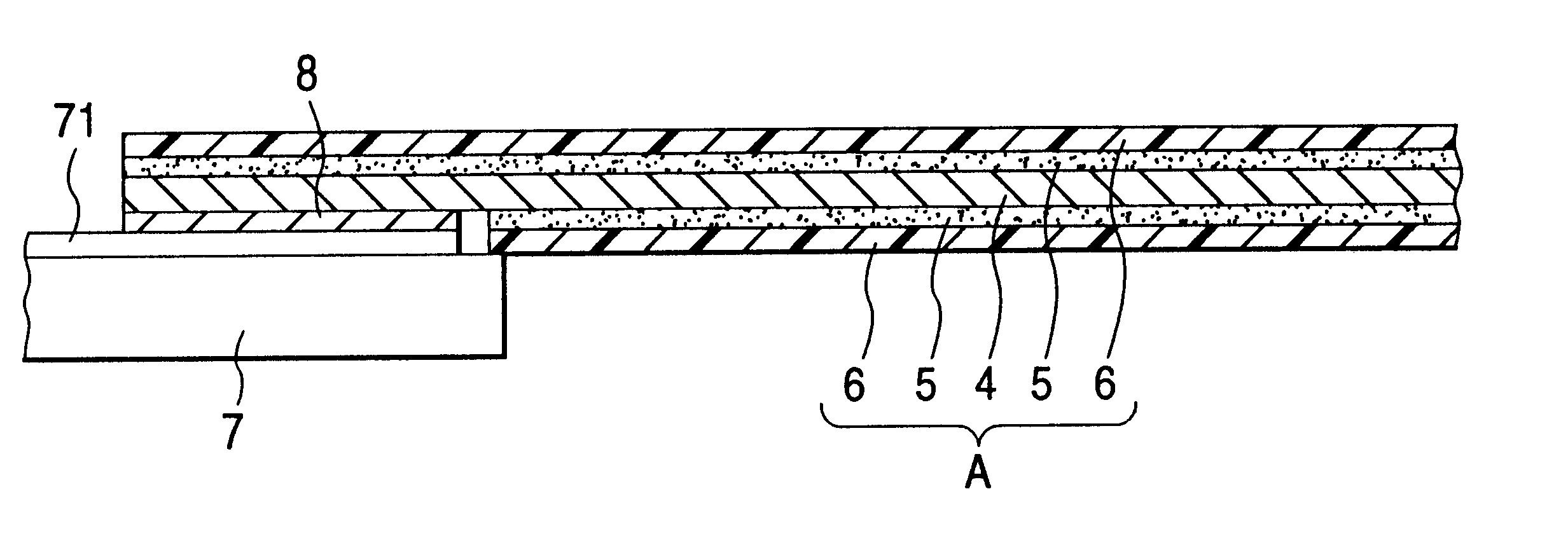
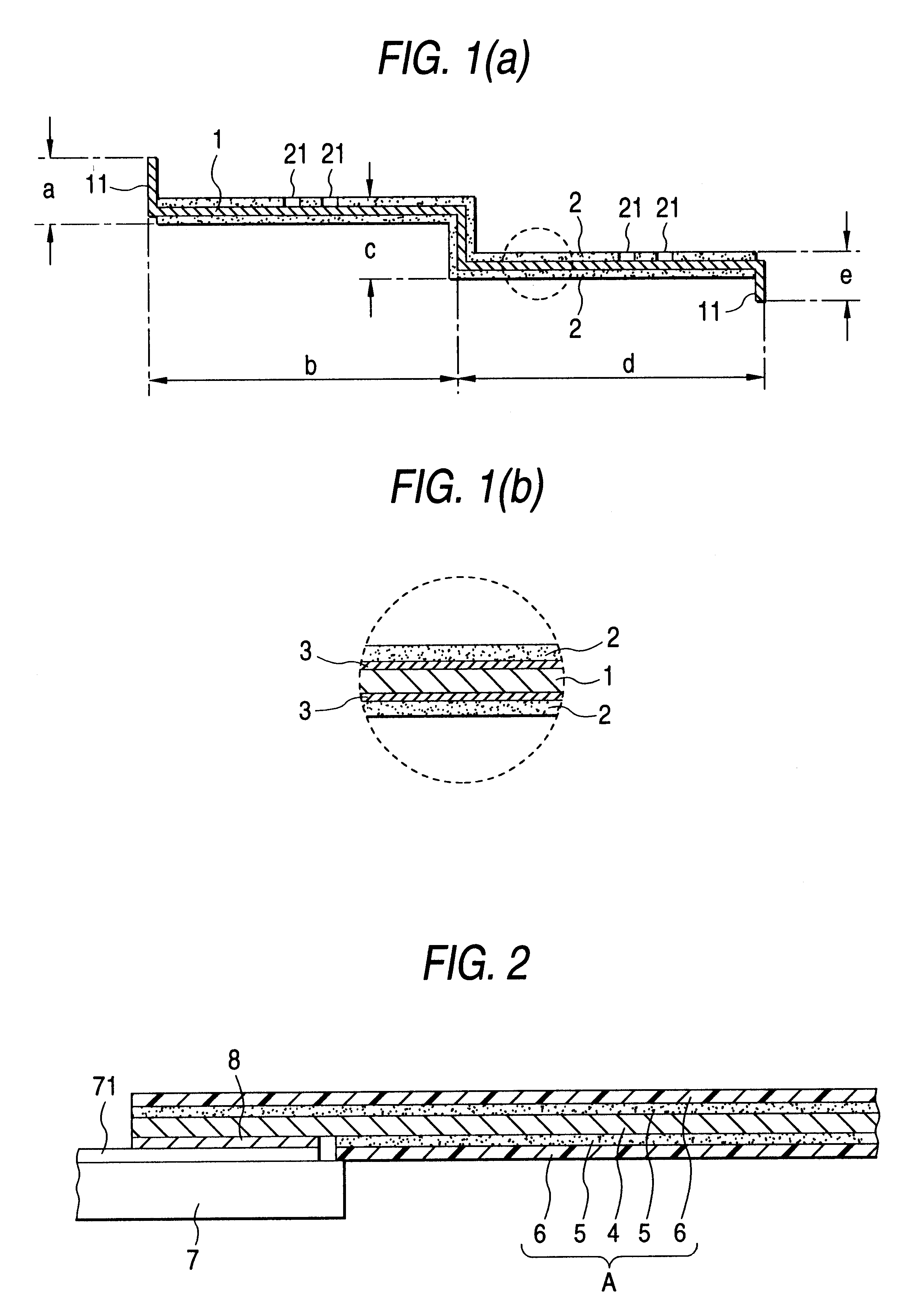
A copper plate having a thickness of 35 .mu.m was stuck to one side of the same polyethylene naphthalate film as used in Example 1 with the same adhesive as used in Example 1 under a heat press (thickness of adhesive layer: 25 .mu.m; heat press condition: 160.degree. C..times.30 kg / cm.times.60 minutes) in the same manner as in Example 1. An etching resist was then formed on the copper plate. The copper plate was then etched with an etching solution to form a circuit conductor having the same pattern as in Example 1. Holes for soldering electronic parts were then made in the same polyethylene naphthalate film having a thickness of 25 .mu.m as used in Example 1. An adhesive layer having a thickness of 25 .mu.m made of a polyester and an isocyanate was then provided on one side of the polyethylene naphthalate film. The polyethylene naphthalate film with an adhesive layer was then heat-pressed onto the foregoing circuit conductor in the same manner as in Example 1. The laminate was then...
example 3
A nickel plate having a thickness of 100 .mu.m was subjected to punching on a mold in a predetermined pattern to obtain a circuit conductor.
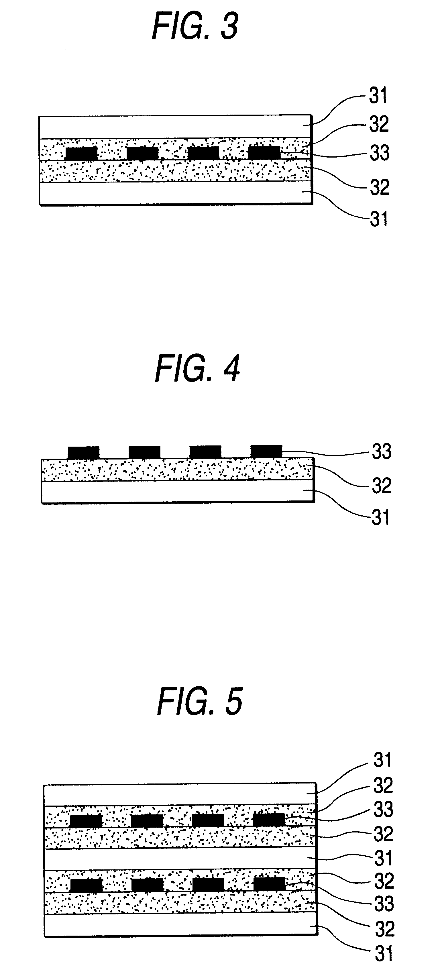
An adhesive layer having a thickness of 25 .mu.m, which was made from a polyester and an isocyanate, was then provided on one side of a polyethylene naphthalate film having a thickness of 25 .mu.m (KALADEX, produced by ICI). The circuit conductor which had been cleaned with a detergent was then interposed between two sheets of the polyethylene naphthalate films with an adhesive. Lamination was effected under a heat press of 30 kg / cm at a temperature of 160.degree. C. for 60 minutes to obtain a circuit board.
example 4
A copper plate having a thickness of 35 .mu.m was stuck to one side of the same polyethylene naphthalate film as used in Example 3 with the same adhesive as used in Example 3 under a heat press (thickness of adhesive layer: 25 .mu.m; heat press condition: 160.degree. C..times.30 kg / cm.times.60 minutes) in the same manner as in Example 3. An etching resist was then formed on the copper plate. The copper plate was then etched with an etching solution to form a circuit conductor having the same pattern as in Example 3. An adhesive layer having a thickness of 25 .mu.m, which was made of a polyester and an isocyanate, was then provided on one side of the same polyethylene naphthalate film as used in Example 3. The polyethylene naphthalate film with an adhesive layer was then heat-pressed onto the foregoing circuit conductor in the same manner as in Example 3 to obtain a circuit board.
PUM
| Property | Measurement | Unit |
|---|---|---|
| Temperature | aaaaa | aaaaa |
| Fraction | aaaaa | aaaaa |
| Linear density | aaaaa | aaaaa |
Abstract
Description
Claims
Application Information
 - Generate Ideas
- Intellectual Property
- Life Sciences
- Materials
- Tech Scout
- Unparalleled Data Quality
- Higher Quality Content
- 60% Fewer Hallucinations
Browse by: Latest US Patents, China's latest patents, Technical Efficacy Thesaurus, Application Domain, Technology Topic, Popular Technical Reports.
© 2025 PatSnap. All rights reserved.Legal|Privacy policy|Modern Slavery Act Transparency Statement|Sitemap|About US| Contact US: help@patsnap.com


