Cached synchronous DRAM architecture having a mode register programmable cache policy

a cache policy and synchronous dram technology, applied in the field of caching sdram and caching policy, can solve the problems of only useful features, unable to and standard sdram does not improve the initial latency of page hits or misses

Inactive Publication Date: 2001-09-11
IBM CORP +2
View PDF1 Cites 106 Cited by
  • Summary
  • Abstract
  • Description
  • Claims
  • Application Information

AI Technical Summary

Problems solved by technology

While standard synchronous DRAMS are designed to be flexible through programmability and to provide higher burst rates not achievable with asynchronous DRAMs, unfortunately, a standard SDRAM does not improve the initial latency of a page hit or miss.
Furthermore, the standard SDRAM does not reduce the penalties caused by the DRAM cycle time (t.sub.RC) and the DRAM precharge time (t.sub.RP).
However, this feature is only useful if the data being stored is orderly and can be organized such that the SDRAM can ping-pong between the two open banks uninterrupted.
With today's multi-tasking computer operating systems, this is a formidable task.
Standard SDRAMs thus suffer some performance limitations including, for instance, an inability to fully utilize the memory bandwidth and further having undesirable system wait states for all memory accesses.

Method used


Image

  • Cached synchronous DRAM architecture having a mode register programmable cache policy
  • Cached synchronous DRAM architecture having a mode register programmable cache policy
  • Cached synchronous DRAM architecture having a mode register programmable cache policy

Examples


Embodiment Construction

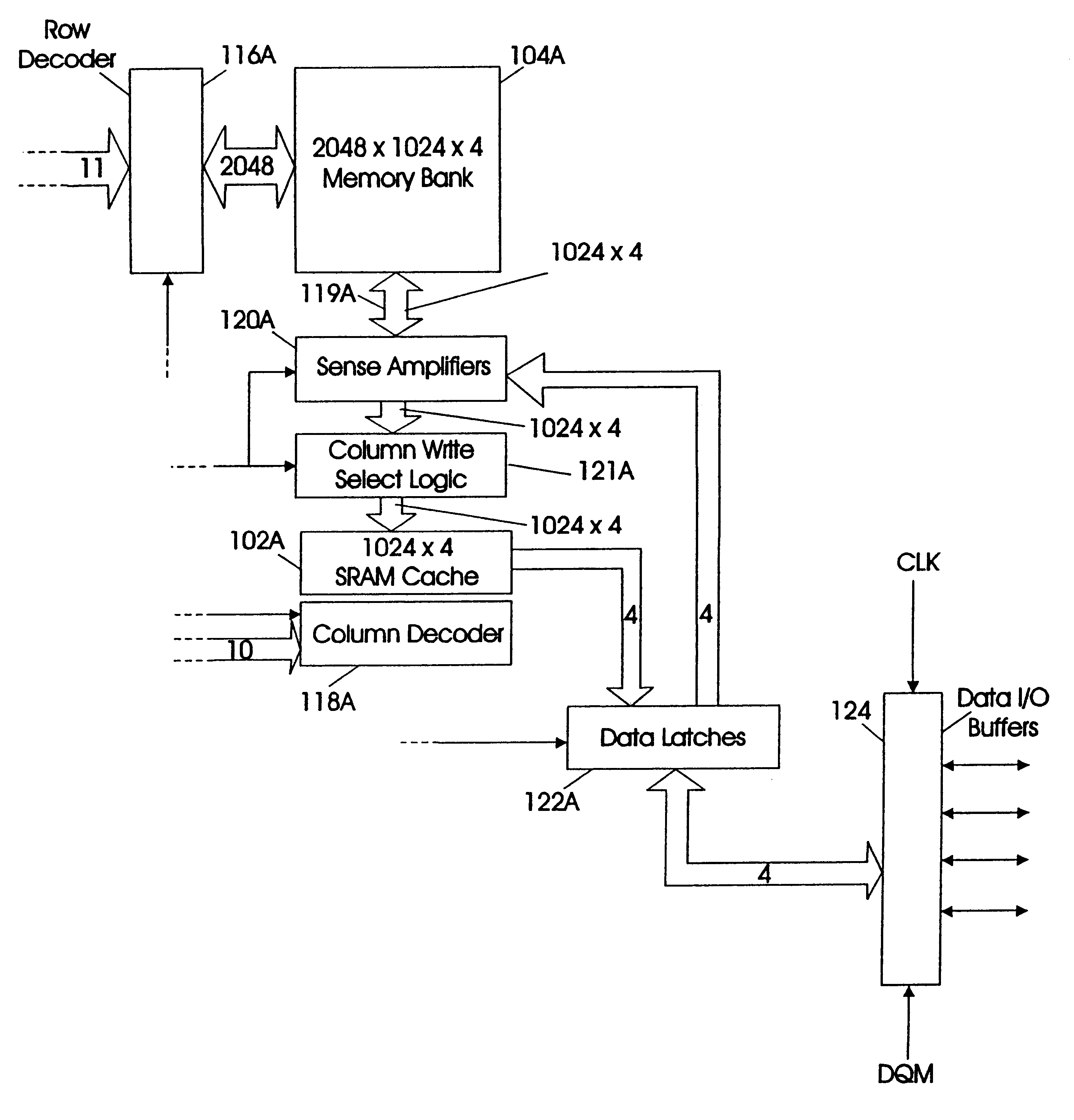
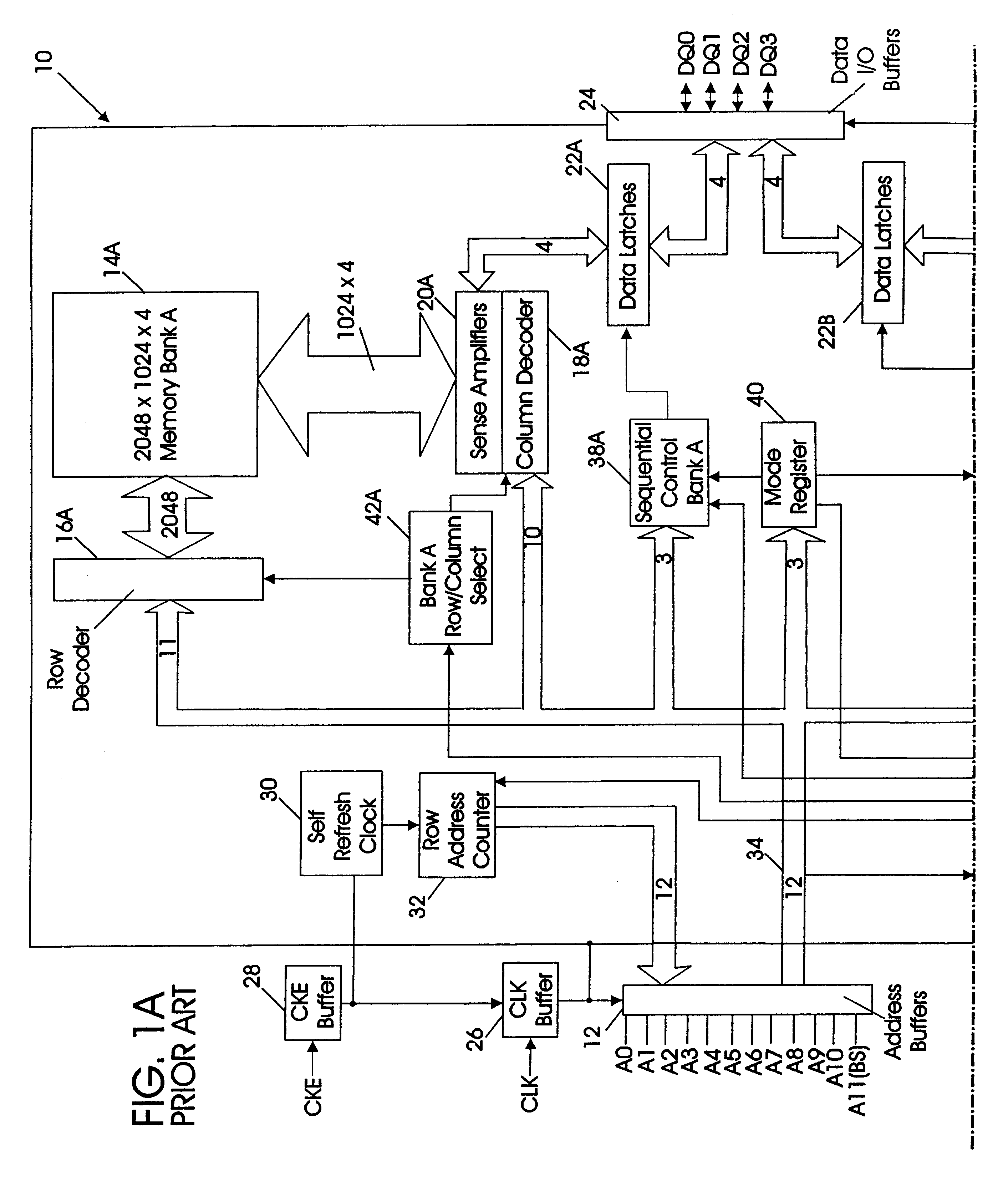
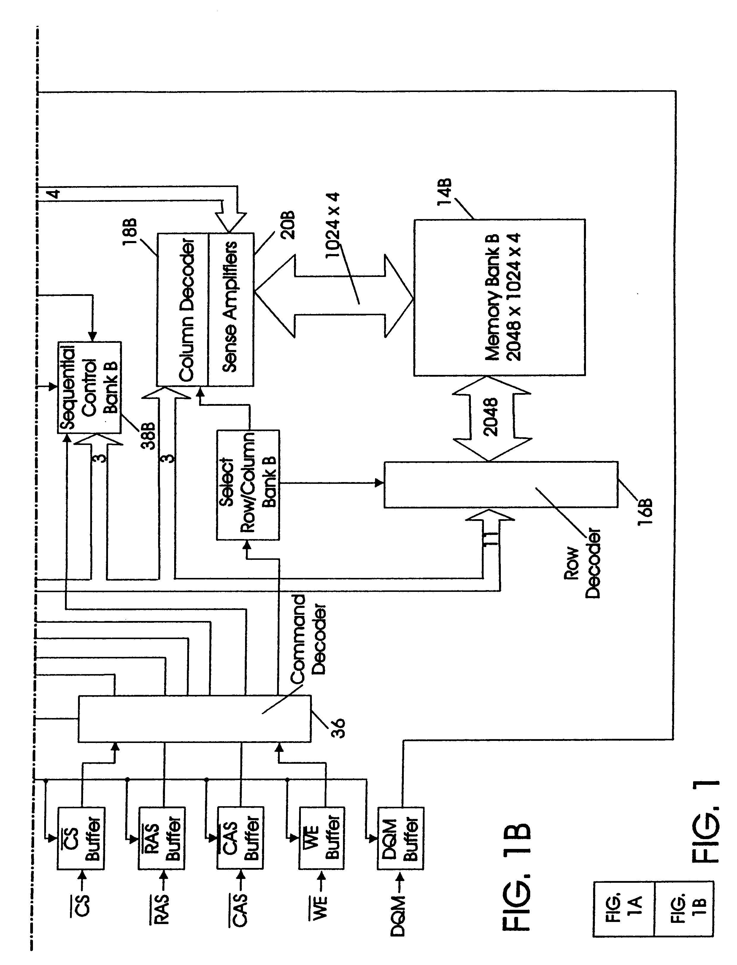
Because dynamic random access memories (DRAMs), and more particularly, synchronous DRAMs are known in the art, the present invention shall be described in particular to elements forming part of, or cooperating directly with, the invention. It is to be understood, however, that other elements not specifically shown or described may take various forms known to persons of ordinary skill in the semiconductor memory art. In addition, for clarity purposes, the present invention shall be described with respect to a 16Mbit SDRAM (2Mbit.times.4 I / O.times.2 Bank). Other SDRAM densities, organizations, and bank quantities are possible.

Referring now to FIG. 3, a block diagram of a cached SDRAM 100 according to the present invention is shown. An 8K bit integrated cache on the SDRAM 100 comprises a 4Kbit integrated static random access memory (row register) (102A, 102B) for each SDRAM bank (104A, 104B). As used in the following, the terms "cache," "integrated row register," and "static random acc...


PUM


Abstract

A cached synchronous dynamic random access memory (cached SDRAM) device having a multi-bank architecture and a programmable caching policy includes a synchronous dynamic random access memory (SDRAM) bank, a synchronous static randomly addressable row register, a select logic gating circuit, and mode register for programming of the cached SDRAM to operate in a Write Transfer mode corresponding to a Normal Operation mode of a standard SDRAM during a Write cycle, and to operate in a No Write Transfer mode according to an alternate operation mode during a Write cycle, thereby operating under a first and a second caching policy, respectively. The SDRAM includes a row decoder for selecting a row of data in a memory bank array, sense amplifiers for latching the row of data selected by the row decoder, and a synchronous column selector for selecting a desired column of the row of data. The row register stores a row of data latched by the sense amplifiers and the select logic gating circuit, disposed between the sense amplifiers and the row register, selectively gates the row of data present on the bit lines to the row register in accordance to particular synchronous memory operations being performed.

Description

1. Field of the InventionThis invention relates generally to synchronous dynamic random access memory (SDRAM) device and, more particularly, to a cached SDRAM and a caching policy thereof.2. Discussion of the Related ArtTurning now to FIG. 1, a block diagram of a standard SDRAM is shown, in particular, a 2Mbit.times.4 I / O.times.2 Bank SDRAM. Other configurations of SDRAMs are also known (e.g., 1Mbit.times.8 I / O.times.2 Bank, 512Mbit.times.16 I / O.times.2 Bank, etc.). The typical SDRAM 10 includes an address buffer 12, first and second memory banks (14A, 14B) and corresponding row decoders (16A, 16B), column decoders (18A, 18B), sense amplifiers (20A, 20B), and data latches (22A, 22B). Data input / output buffers 24 receive data to be written into a memory array (i.e., either array 14A or 14B) and output data read from a memory array (i.e., either array 14A or 14B).An externally supplied system clock (CLK) signal is input to a clock buffer 26 (CLK Buffer), the CLK signal for providing s...

Claims


Application Information

Patent Timeline
Patent Type & Authority Patents(United States)
IPC IPC(8): G06F12/08G11C11/407G11C11/401G11C11/409
CPCG06F12/0893G06F12/0804G11C11/407
Inventor ROGERS, JIM L.TOMASHOT, STEVEN W.BONDURANT, DAVID W.JONES, JR., OSCAR FREDERICKMOBLEY, KENNETH J.
Owner IBM CORP
Why Eureka
Try Eureka