Sputter deposition utilizing pulsed cathode and substrate bias power

a technology of pulsed cathode and substrate, which is applied in the direction of sputtering coating, vacuum evaporation coating, coating, etc., can solve the problems of limited sputtering power supply output, etc., to achieve a three-fold increase in transport speed and a ten-fold increase in sputtering power

Inactive Publication Date: 2001-09-18
SEAGATE TECH LLC
View PDF12 Cites 97 Cited by
  • Summary
  • Abstract
  • Description
  • Claims
  • Application Information

AI Technical Summary

Benefits of technology

An advantage of the present invention is an improved method for sputter...

Problems solved by technology

However, practical limitations exist with respect to increasing the deposition speed obtainable with conventional sputtering apparatus and manufacturing technology, whether the deposition is performed onto static or moving substrates.
For example, the available technology imposes certain limits on the output of RF and DC sputter power supplies and transport speed of the substrates from one process chamber to another (via air-locks, etc.).
More specifically, available technology cannot provide more than about a ten-fold ("10.tim...

Method used


Image

  • Sputter deposition utilizing pulsed cathode and substrate bias power
  • Sputter deposition utilizing pulsed cathode and substrate bias power
  • Sputter deposition utilizing pulsed cathode and substrate bias power

Examples


Embodiment Construction

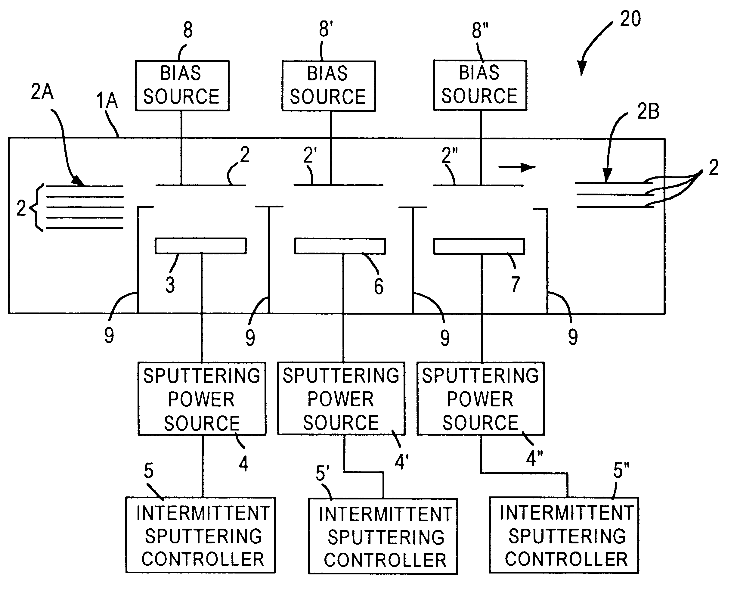
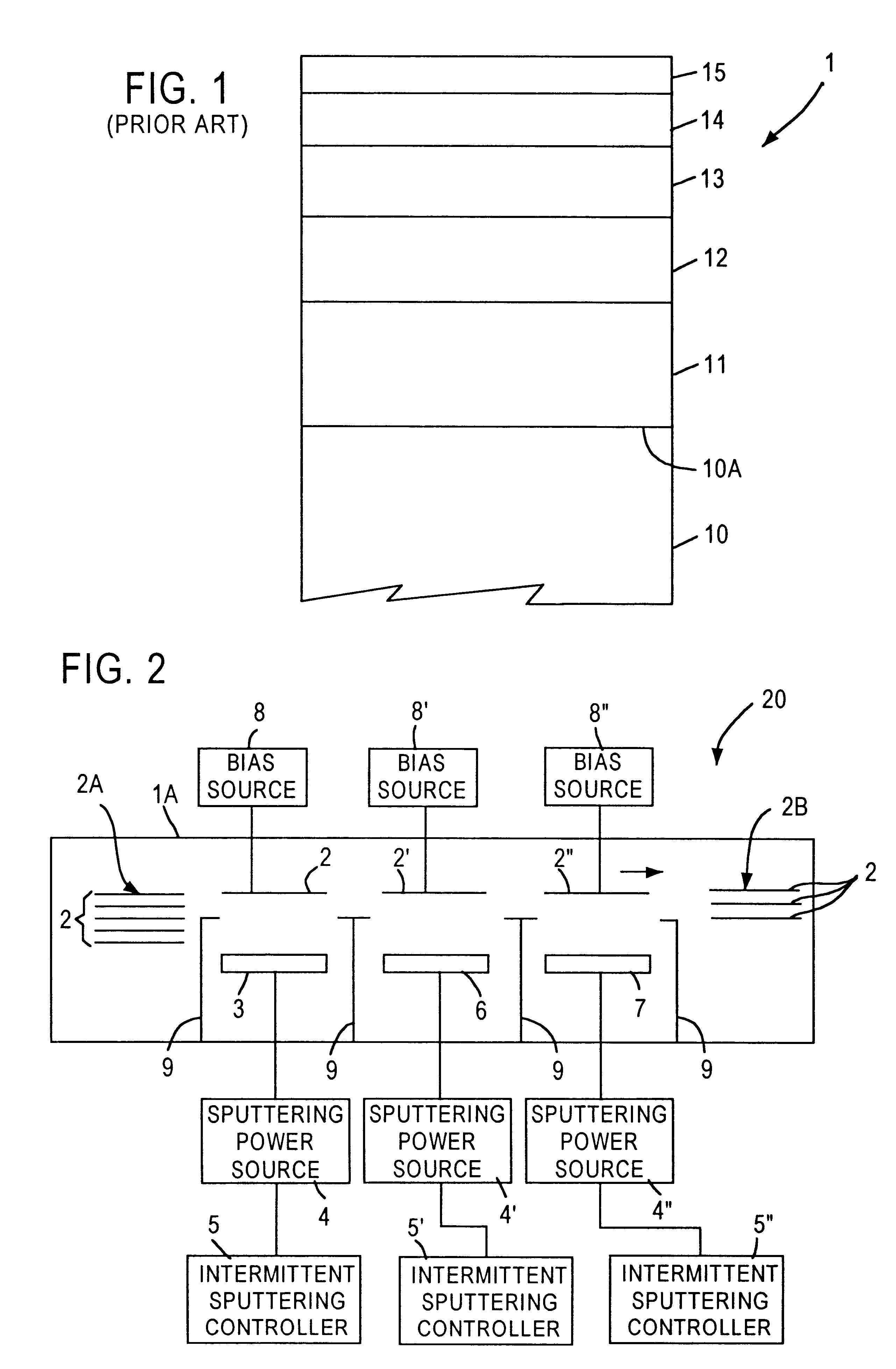
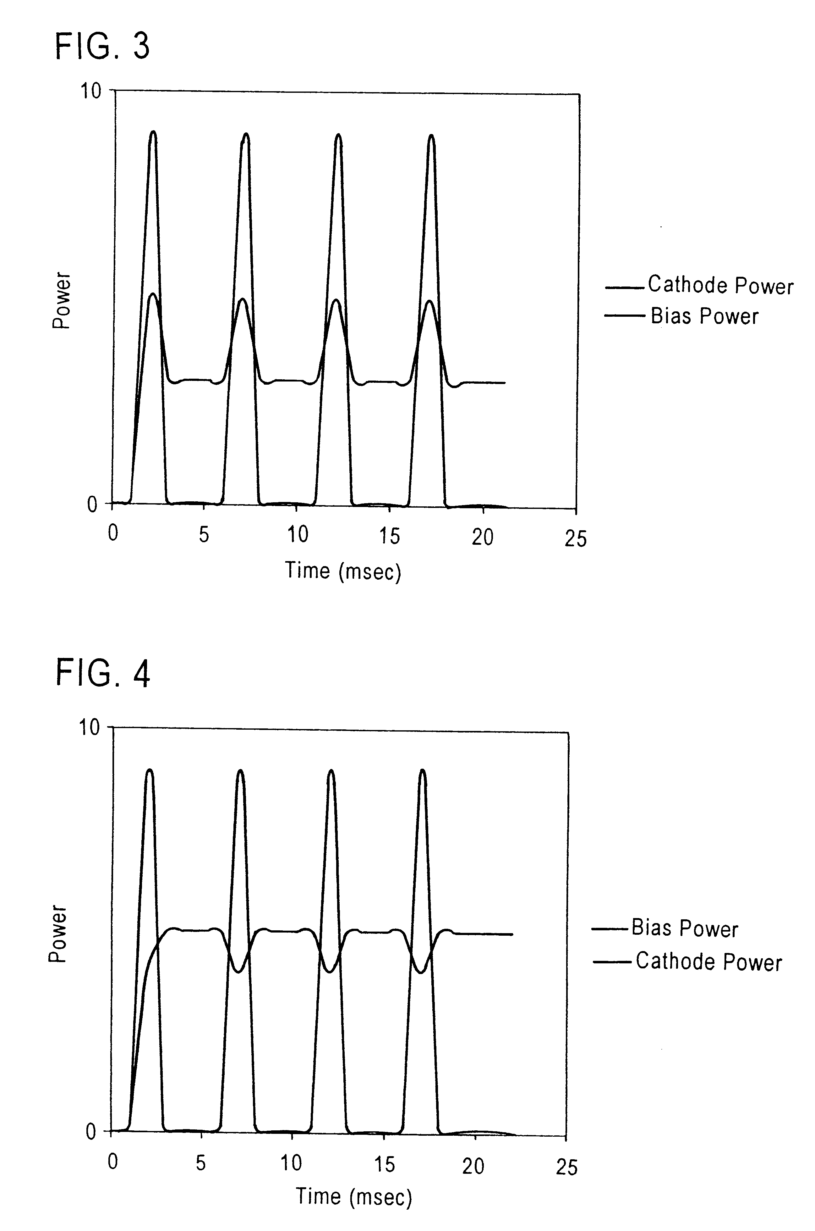
The present invention is based upon the recognition that the above-described limitations / restrictions imposed upon high rate deposition of high purity thin film layers onto static or moving substrates by, e.g., power supply output and substrate transport speed considerations, can be avoided by delivering to the respective cathode / sputtering target assemblies high-power, negative polarity pulses of limited duration to effect target sputtering such that the average deposition rate of the respective thin film remains close to that utilized in conventional sputter deposition processing. According to the invention, a sufficient number of negative polarity pulses of a preselected power level is applied to each of the cathode / target assemblies to sputter deposit on the substrate respective thin film layers of desired or requisite thicknesses. An advantage provided by the inventive methodology is that, in the case of deposition onto moving substrates, the line speed of substrate transport c...


PUM

PropertyMeasurementUnit
Thicknessaaaaaaaaaa
Polarityaaaaaaaaaa
Electric potential / voltageaaaaaaaaaa

Abstract

A method for depositing on a substrate surface a thin film layer comprising a target material comprises providing a cathode including a target having a sputtering surface comprised of the target material, with the target sputtering surface facing the substrate surface with a space therebetween, and sputtering the target material onto the substrate surface by applying a plurality of negative voltage pulses to the cathode while simultaneously applying a bias voltage to the substrate. Embodiments include depositing thin film layers onto static or moving substrates and application of constant or time-varying substrate bias voltage. The invention finds particular utility in the formation of high purity layers in the automated manufacture of magnetic data/information storage and retrieval media.

Description

The present invention relates to a method for performing high-rate cathode sputtering of a target material for obtaining high purity thin film layers on substrate surfaces. More particularly, the invention relates to a method for performing high-rate sputter deposition onto static or moving substrates to obtain high purity thin film layers having desired physical, chemical, and / or mechanical properties. The invention has particular utility in the manufacture of magnetic recording media comprising a layer stack or laminate of a plurality of overlying layers.Magnetic recording media are widely employed in various applications, particularly in the computer industry for data / information storage and retrieval purposes. A conventional, single-sided, longitudinal magnetic recording medium 1 in e.g., disk form, such as utilized in computer-related applications, is schematically depicted in FIG. 1 and comprises a non-magnetic substrate 10, e.g., of glass, ceramic, glass-ceramic composite, po...

Claims


Application Information

Patent Timeline
IPC IPC(8): C23C14/56C23C14/34
CPCC23C14/34C23C14/568C23C14/345
Inventor MCLEOD, PAUL STEPHEN
Owner SEAGATE TECH LLC
Why Eureka
Try Eureka