

Circuit and method of fabricating a memory cell for a static random access memory
a memory cell and random access memory technology, applied in the field of memory cells, can solve the problems of affecting the performance of the corresponding transistor formed, the potential for misalignment between the layers of semiconductor materials defining the sram memory cell transistors, and the disadvantageous increase of the size of the memory cell
- Summary
- Abstract
- Description
- Claims
- Application Information
AI Technical Summary
Problems solved by technology
Method used
Image

Examples
Embodiment Construction
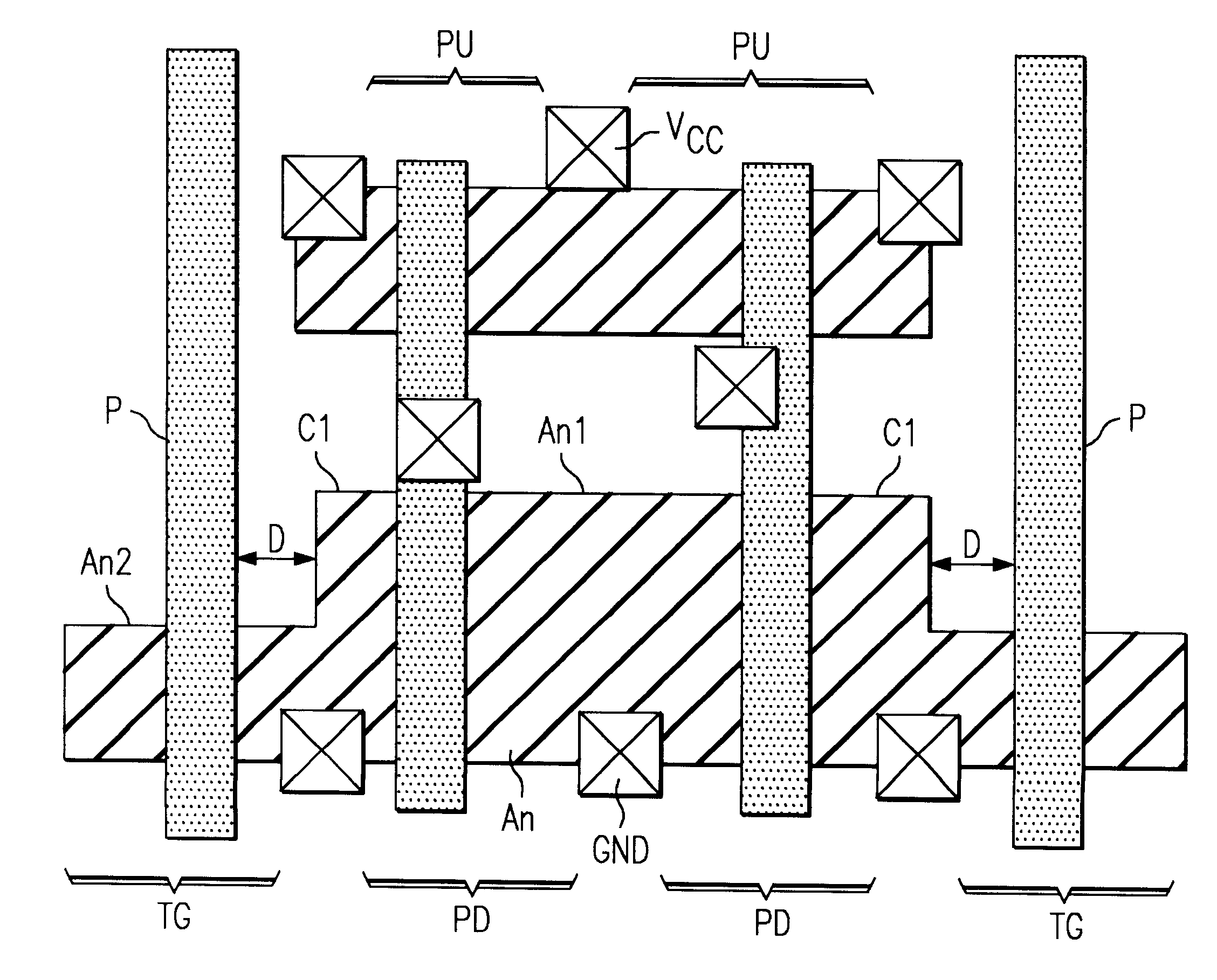
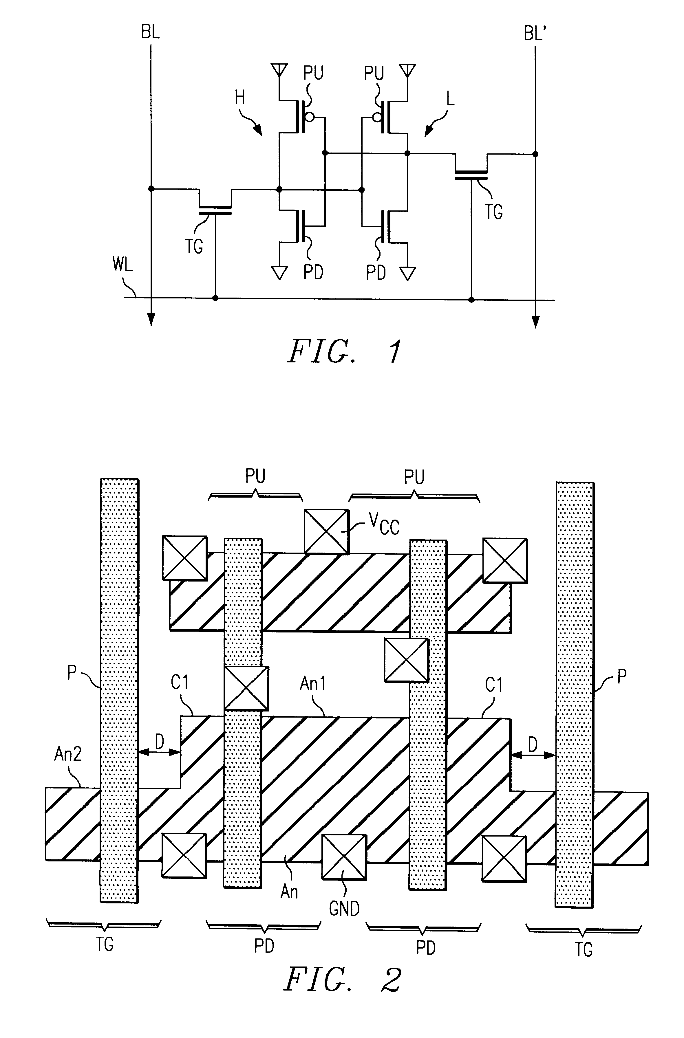
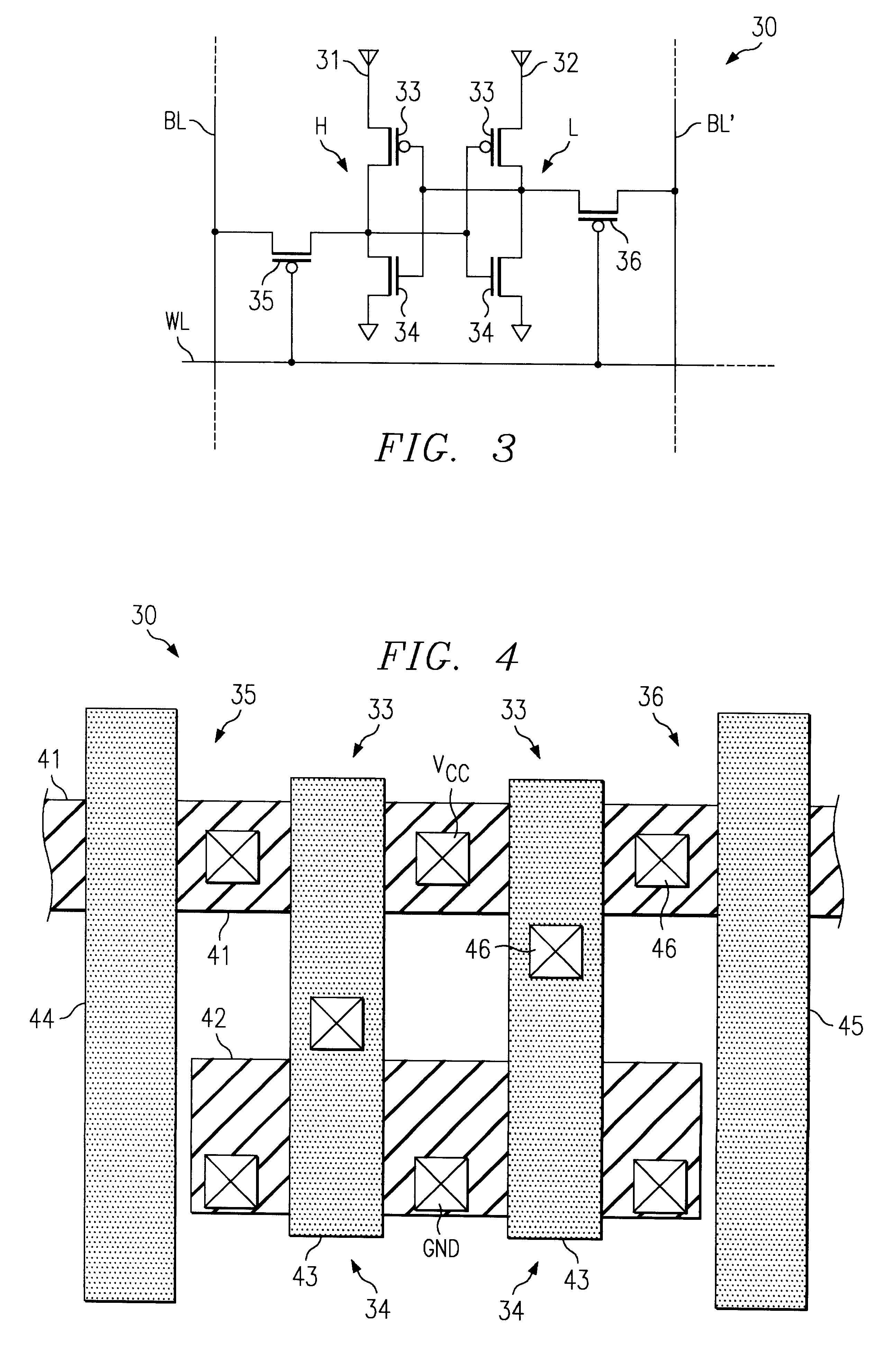
Referring to FIGS. 3-4, there is shown a memory cell 30 for a static random access memory (SRAM) device according to a preferred embodiment of the present invention. The memory cell 30 is adapted to improve the yield and scalability of the SRAM device by substantially eliminating the adverse effects due to round-off and misalignment between semiconductor layers forming the transistors of the SRAM memory cells.
Memory cell 30 includes two conventional logic inverters 31 and 32 that are cross-coupled to each other to form a latch. The cross-coupled inverters 31 and 32 are selectively set to store data representing either a high or low logic level. Each logic inverter is formed from a p-channel pull-up MOS transistor 33 and an n-channel pull-down MOS transistor 34. In addition, memory cell 30 includes two transmission gate transistors 35 and 36 that provide access to cross-coupled inverters 31 and 32. Transmission gate transistors 35 and 36 are each p-channel MOS transistors.
In order to...
PUM
 Abstract
Description
Claims
Application Information