Wiring arrangement including capacitors for suppressing electromagnetic wave radiation from a printed circuit board

a technology of electromagnetic wave radiation and wiring arrangement, which is applied in the direction of electrical apparatus construction details, line-transmission details, final product manufacture, etc., can solve the problems of large alterations to the structure of the board, and inability to achieve sufficient suppression of power source voltage variation

Inactive Publication Date: 2001-10-02
NEC CORP
View PDF10 Cites 35 Cited by
  • Summary
  • Abstract
  • Description
  • Claims
  • Application Information

AI Technical Summary

Problems solved by technology

With the demand of high speed operation and high integration of electronic devices, unnecessary electromagnetic wave radiation occurs from a device of which a function is not to radiate the electromagnetic waves, to raise public concern.
However, even if the power source layer and a part of the ground planar layer are so disposed that they are close to each other in the printed circuit board shown in FIG. 1, the increase of the electrostatic capacity obtained thereby is extremely small and the sufficient suppression of the power source voltage variation cannot be expected.
All the above prior arts unavoidably require large alterations to the board structures.
However, in a frequency band between 30 MHz and 1 GHz in which the radiation of the unnecessary electromagnetic waves raises the public concern (controlled frequency band), the capacitor element ZC shown in FIG. 4 cannot be regarded as a mere capacitor because of its parasitic inductance.
However, in this structure, a plurality of the first capacitors must be mounted along the periphery of the circuit board, and when a large circuit board is to be employed, the number of the capacitors required becomes large.
However, the .pi.-type filter containing the ferrite beads is expensive to invite the cost increase of the printed circuit board.

Method used


Image

  • Wiring arrangement including capacitors for suppressing electromagnetic wave radiation from a printed circuit board
  • Wiring arrangement including capacitors for suppressing electromagnetic wave radiation from a printed circuit board
  • Wiring arrangement including capacitors for suppressing electromagnetic wave radiation from a printed circuit board

Examples


embodiment 1

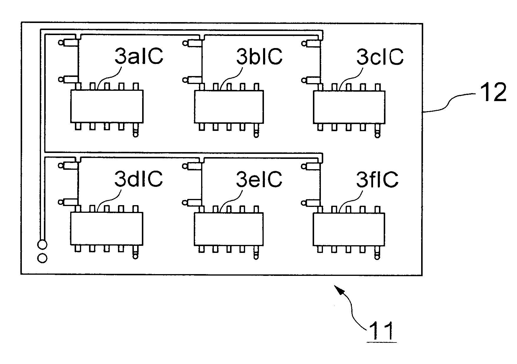
In FIGS. 11 to 13, a circuit printed board 11 has at least one signal layer 12 and at least one ground layer 25, and the signal layer 12 has several ICs (3a to 3f IC). A capacitor 17a is located near a power supply terminal 16a of the respective ICs.

The capacitor 17a in FIG. 12 has one terminal connected with the power supply terminal 16a and the source line 19a and the other terminal connected with the ground layer 25 through a via hole 18a. Another capacitor 20a is located at the top end of this source line 19a. The capacitor 20 has one terminal connected with the source line 19a and a common source line 22 for supplying power to an active element on the whole board and the other terminal connected with the ground layer 25 through a via hole 21a. A ground terminal 23a of IC is connected with the ground layer 25 through a via hole 24a. The ground layer 25 is formed of conductors.

The capacitors 17a and 20a have a capacity of 0.001 .mu.F or more, and are desirably components having a...

embodiment 2

FIG. 18 shows a second embodiment of a printed circuit board in accordance with the present invention. In this embodiment, the description of the same elements as those of the first embodiment will be omitted by affixing the same numerals thereto.

This mounting structure is characterized by the reduction of the number of capacitors by jointly sharing the capacitor 17e mounted near the adjacent power supply terminals in place of employing the capacitor 20e shown in FIG. 17. A capacitor 17f shown in FIG. 18 is employed to have the same function as that of the capacitor 20e in FIG. 17. The width and the length of the source line between adjacent capacitors, more in concrete, those of the source line 19e, 19f, 19g and 19h between the capacitors 17e and 17f, between the capacitors 17f and 17g, between the capacitors 17g and 17h and between the capacitors 17h and 20e, respectively, are determined in accordance with the above method of designing the width (W) and the length (L) of the sourc...


PUM


Abstract

Disclosed herein is a printed circuit board comprising a ground layer and a signal layer in which the characteristic impedance of a specific source line is made to be not less than three times as large as the impedance at an upper limit frequency at which the electromagnetic wave radiation of a specific capacitor may occur. In this printed circuit board, variation of a power source voltage and unnecessary electromagnetic wave radiation can be suppressed.

Description

(a) Field of the InventionThe present invention relates to a printed circuit board constituting a part of an electronic device, more in particular, to the printed circuit board for suppressing unnecessary electromagnetic waves radiated therefrom.(b) Description of the Related ArtWith the demand of high speed operation and high integration of electronic devices, unnecessary electromagnetic wave radiation occurs from a device of which a function is not to radiate the electromagnetic waves, to raise public concern. Therefore, the unnecessary electromagnetic waves, especially those of 30 MHz to 1 GHz, must be legally controlled. Manufacturers of the electronic devices are requested to design and manufacture articles satisfying this legal standard.In order to suppress the unnecessary electromagnetic wave radiation from the electronic devices, it is most effective that the radiation is suppressed at a printed circuit board in the device. Conventionally, a number of printed circuit boards ...

Claims


Application Information

Patent Timeline
Patent Type & Authority Patents(United States)
IPC IPC(8): H05K9/00H05K1/02
CPCH05K1/0231H05K9/0066H05K1/023H05K2201/10022H05K2201/10522H05K2201/10636H05K2201/10689Y02P70/50
Inventor SASAKI, HIDEKIHARADA, TAKASHI
Owner NEC CORP
Why Eureka
Try Eureka