Process for fabricating micromechanical devices

a micromechanical device and process technology, applied in the direction of relays, generators/motors, snap-action arrangements, etc., can solve the problems of high vertical resolution (i.e. resolution in the direction normal to the substrate surface) that is more difficult to obtain than planar resolution, and the device will not operate in the intended manner

Inactive Publication Date: 2001-10-09
LUCENT TECH INC
View PDF4 Cites 39 Cited by
  • Summary
  • Abstract
  • Description
  • Claims
  • Application Information

AI Technical Summary

Problems solved by technology

The higher resolution derives from the fact that high vertical resolution (i.e. resolution in the direction normal to the substrate surface) is more difficult to obtain than planar resolution (i.e. resolution in the plane of the layer).
One problem with manufacturing such MEMS devices is that, occasionally, a plate does not release (i.e. pivot away from the substrate) after the sacrificial underlying layer of silicon dioxide has been removed.
If the plates fail to pivot, then the device will not operate in its intended manner.
Applicants have observed that it is difficult to get the hinged members to release consistently.
Because of the non-uniform release of the various members that make up the device, the orientation of the structure during release is not predictable.

Method used


Image

  • Process for fabricating micromechanical devices
  • Process for fabricating micromechanical devices
  • Process for fabricating micromechanical devices

Examples


Embodiment Construction

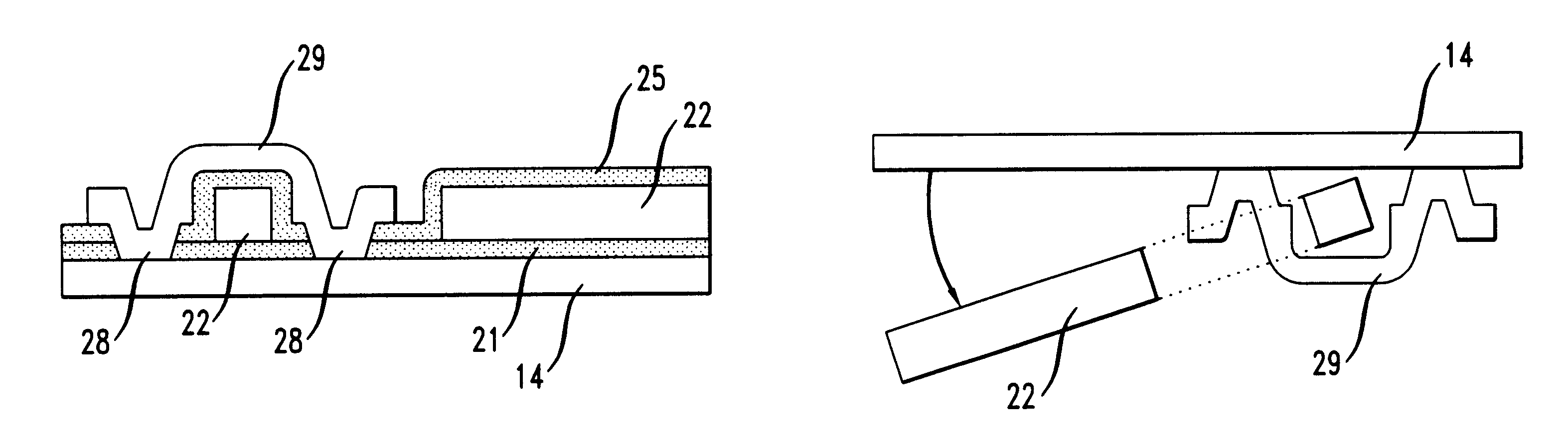
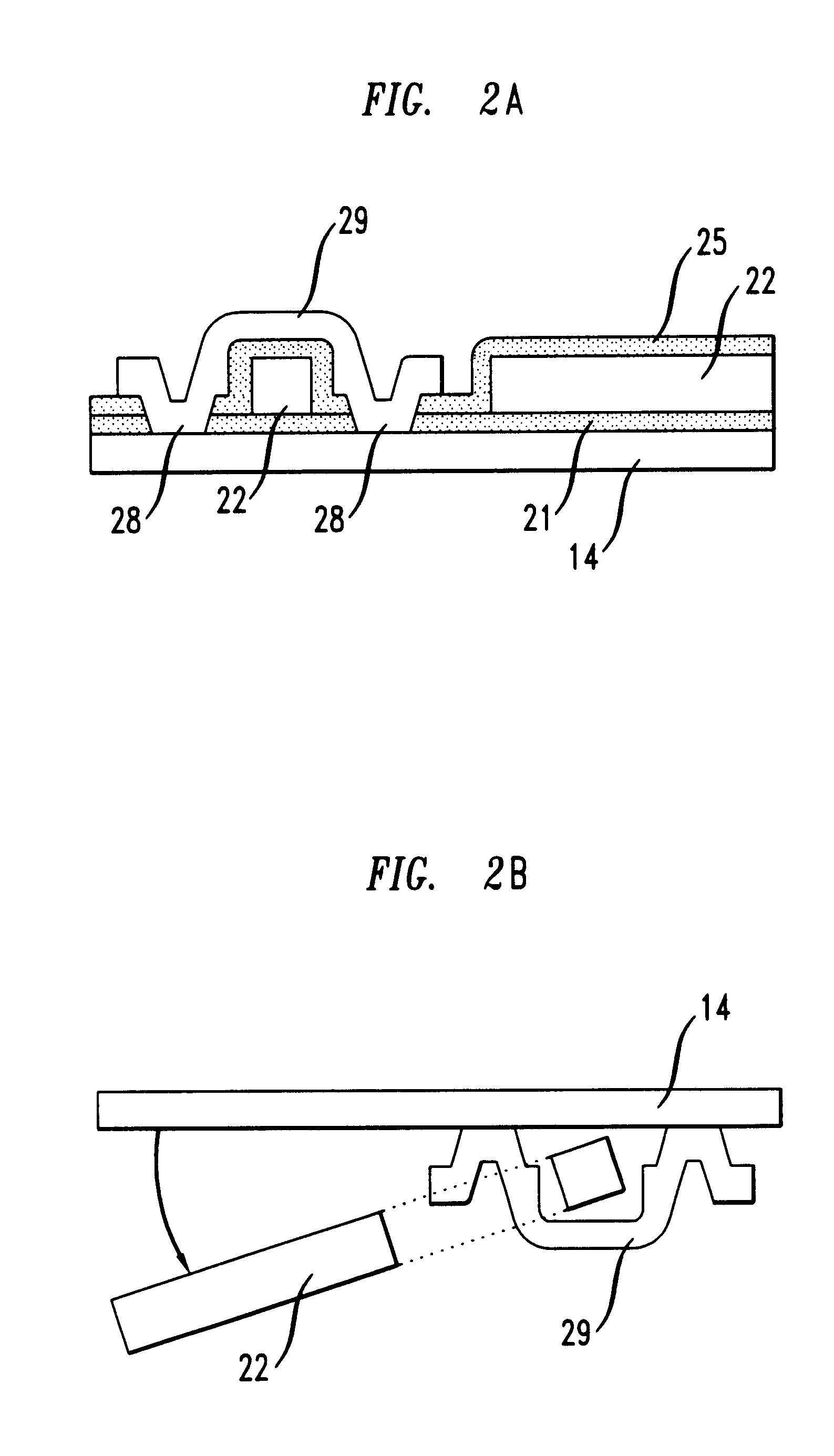
In this example, a hinged plate was released according to the process of the present invention. This example is described with reference to FIG. 5. Specifically, substrates 101 with a plurality of structures 105 having hinged plates (not shown) similar to those depicted in FIG. 3 were placed in a chip-carrier 110 and locked into position. The chip-carrier 110 was seated onto a chamber 120 such that the substrate was suspended in the chamber 120 face down. The chamber 120 was affixed to a base 135. The base had an inlet 140 in fluid communication with the chamber inlet 125. The base also had a drain 145 for draining away the overflow from the chamber 120. The chamber 120 was equipped with an inlet 125 and an overflow 130 for flowing fluids through the chamber 120. Low frequency (i.e. 50-60 Hz in the vertical direction) agitation was provided to the chamber 120. For these examples the vertical displacement was varied between about 100 .mu.m and 450 .mu.m.

The shaker control was turned ...


PUM

PropertyMeasurementUnit
frequencyaaaaaaaaaa
vertical displacementaaaaaaaaaa
frequencyaaaaaaaaaa

Abstract

A process for fabricating a MEMS device is disclosed. The device has at least one hinged element. The MEMS device including the hinged element is delineated and defined on a semiconductor substrate. The substrate is placed device side down in a chamber. The MEMS device is then exposed to a release expedient for sufficient amount of time for the release expedient to dissolve a sacrificial material connecting the element to the substrate. Upon the dissolution of the sacrificial material, the element is released from the substrate and pivots away from the surface.

Description

The present invention relates generally to processes for fabricating micromechanical devices, and more particularly, micro-electro-mechanical systems (MEMS) that are components of optical communication systems.DESCRIPTION OF THE RELATED ARTMEMS devices are miniature mechanical devices that are controlled by electrical or optical signals. Such devices have dimensions that are typically less than one millimeter, with some dimensions being on the order of one micron or less. In order to fabricate mechanical devices on this size scale, microfabrication techniques have been developed.Microfabrication techniques for MEMS devices utilize the lithographic techniques used to fabricate semiconductor integrated circuits. In integrated circuit fabrication, a layer or layers of material are deposited on a substrate (typically a semiconductor substrate with one or more layers of material formed thereon). Lithography is then used to pattern the layer or layers into the desired shape. In lithograph...

Claims


Application Information

Patent Timeline
Patent Type & Authority Patents(United States)
IPC IPC(8): B81B5/00B81C1/00
CPCB81C1/00198Y10S438/924
Inventor DECKER, ROBERT LEROYKUCK, VALERIE JEANNEPACZKOWSKI, MARK ANTHONYSIMPKINS, PETER GERALD
Owner LUCENT TECH INC
Why Eureka
Try Eureka