Semiconductor device having high density interconnections and method for manufacturing the same

a technology of high density interconnection and semiconductor devices, which is applied in the direction of semiconductor devices, semiconductor/solid-state device details, electrical apparatus, etc., can solve the problems of short-circuiting with the neighboring bit line, and affecting the operation of the devi

Inactive Publication Date: 2001-10-09
KK TOSHIBA
View PDF5 Cites 98 Cited by
  • Summary
  • Abstract
  • Description
  • Claims
  • Application Information

AI Technical Summary

Problems solved by technology

Though the barrier metal film 111 is prepared to prevent silicon from mutual reaction with tungsten, such as a solid-state reaction called as "contact spiking", which leads to a leakage current, the step coverage is not so good because it is formed by sputtering.
(1) The aspect ratio for the contact hole 110b of the present DRAM is the order of 1.5 to 3 and further has a tendency to be required to have high values more than 4. When the contact hole 110b of DRAM is filled up by the tungsten plug 112, the tungsten film cannot be filled sufficiently into the interior of the contact hole 110b, if the aspect ratio of the contact hole 110b is high. This is due to the fact that the angle between the substrate surface and the side surface of the contact hole, .theta.6 (hereafter denote as "the taper angle"), is nearly a right angle. Consequently, it is hard to bury the tungsten plug 112 into the contact hole 110b uniformly.
(2) As shown in FIG. 3, even if the aspect ratio is reduced, the situation that the angle between the side surface of the contact hole 110a and the bottom surface of the bit line 109, .theta.7 (hereafter the corner having the angle .theta.7 is denoted as "shoulder"), is nearly a right angle (.theta.>87.degree..about.89.degree.) cannot be improved, so that the barrier metal film 111 is hard to be deposited and there is a possibility of a penetration of tungsten plug 112 into silicon through a pinhole of the barrier metal film. That is, the barrier metal film 111 in the shoulder portion of the upper edge of contact hole becomes thick and by this increment of the thickness, the layer thickness at a corner "X" in the bottom surface is extremely reduced, resulting in possibly of a significant intermixing between tungsten plug 112 and silicon substrate 101 at the corner "X".
(3) In order to avoid the above-mentioned problem (2), a technique of increasing the hole diameter of the contact hole 110b only on the upper portion, keeping the diameter constant at the lower portion as shown in FIGS. 5(a) and (b), is proposed. However, in this case there is a possibility of short-circuiting with the neighboring bit line when the bit line spacing becomes narrow.
Particularly, when the contact hole positions of the neighboring wirings approach, there is a possibility of direct interference between the contact holes and so, this restriction is further enlarged.

Method used


Image

  • Semiconductor device having high density interconnections and method for manufacturing the same
  • Semiconductor device having high density interconnections and method for manufacturing the same
  • Semiconductor device having high density interconnections and method for manufacturing the same

Examples


first embodiment

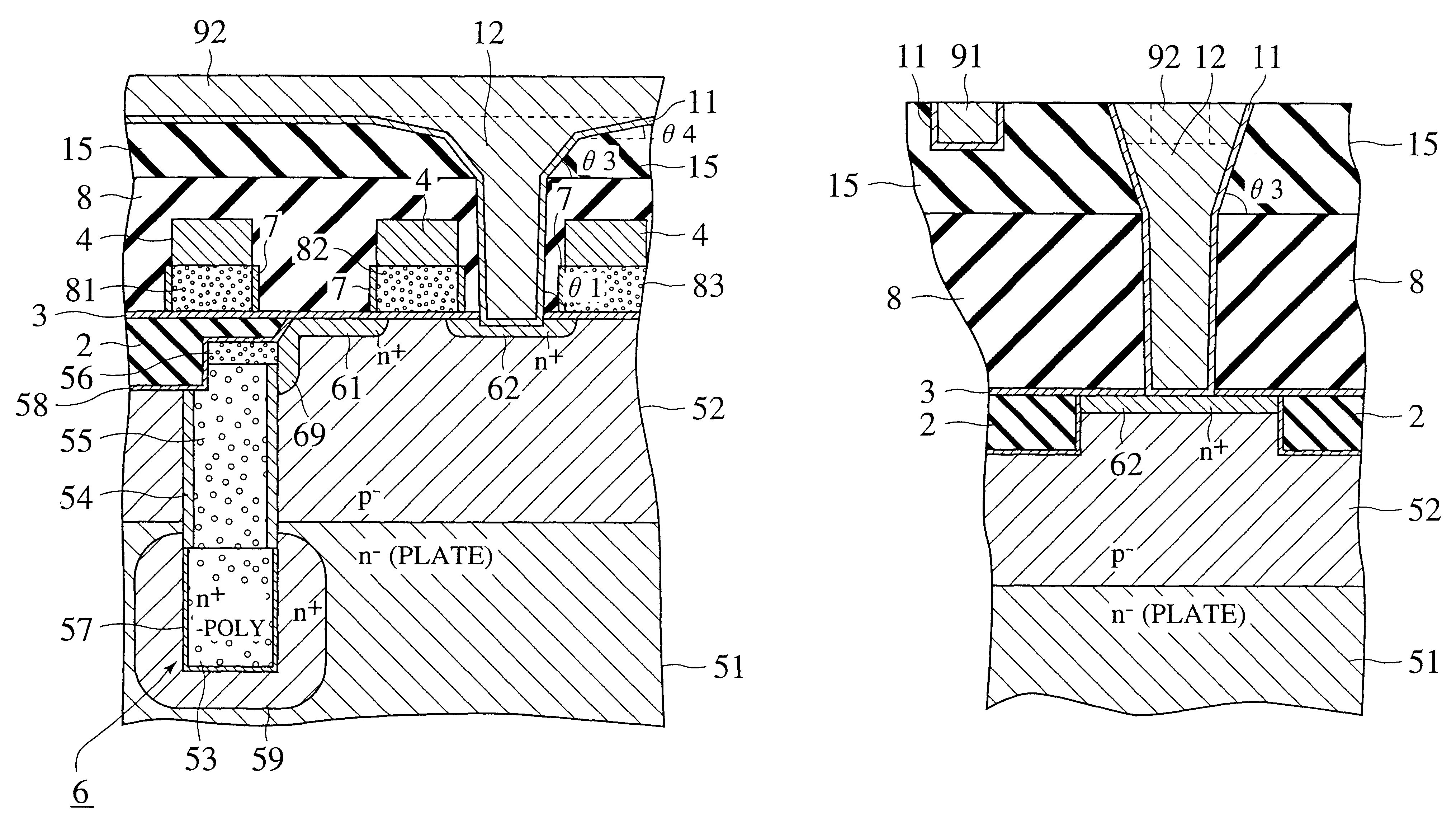
FIGS. 6A and 6B are top plan views of DRAM according to the present invention. FIG. 6B shows the shape of contact plugs 12 and active areas 66 (device regions) by eliminating the bit lines located on the upper level (top layer). FIG. 6C is a cross-sectional view along the I--I direction of FIG. 6A. FIG. 6D is a cross-sectional view along the II--II direction of FIG. 6A.

DRAM according to the first embodiment of the present invention is constructed by arranging a number of memory cells in the form of X-Y matrix. Each memory cell is made of an access transistor and a storage capacitor. FIGS. 6A and 6B are partial diagrams showing only several memory cells among them. FIG. 6C shows the neighborhood of two memory cells to be connected with word lines 82 and 83. The contact plug 12 arranged in the center of two memory cells is connected with a bit line 92 extending right and left. Access transistors comprising n.sup.+ source region 61 and n.sup.+ drain region 62 are arranged on both sides...

second embodiment

FIGS. 19A and 19B show top plan views of a DRAM according to a second embodiment of the present invention. In FIG. 19B, the top layer bit lines have been omitted in order to illustrate the shape of the contact plugs 12 and active areas 66. FIG. 19C is a cross-sectional view along the I--I direction of FIG. 19A; FIG. 19D, a cross-sectional view along the II--II direction of FIG. 19A

As FIG. 19C shows, the DRAM of the second embodiment of the present invention comprises an n.sup.- buried layer 51, which is used as a plate layer, provided on a p-type (100) silicon substrate (not shown in the diagram), and a DRAM unit cell access transistor which is provided on the surface of a p-well 52 above the plate layer. The p-well 52 is surrounded by an insulating film 2, comprising silicon oxide (SiO.sub.2) or the like, for isolating the elements, formed by a method such as STI method, the inner portion thereof forming an active area (in FIG. 19B, the extent of these active areas is indicated by ...

third embodiment

The above explanation described a case where the position of the contact hole and the position of the surface interconnections, such as the bit lines, are correctly aligned. In fact, however, there may be slight deviation from the correct positions within a permissible range. But, it should be clear from the following explanation of a third embodiment that the present invention is able to achieve its objectives even when such deviation exists.

FIG. 33A is a top plan view of a semiconductor device according to a third embodiment of the present invention. And, FIG. 33B is a cross-sectional view taken along I--I direction of FIG. 33A, and FIG. 33C, a cross-sectional view taken along II--II direction of FIG. 33A. As FIG. 33B shows, contact plug 12 juts out asymmetrically at a right angle to the surface interconnections (the II--II direction). As FIGS. 33B and 33C show, the semiconductor device according to the third embodiment of the present invention comprises a transistor on a p-type (...


PUM


Abstract

A main electrode region of a semiconductor element is provided in a semiconductor region on the surface of a semiconductor substrate, and first and second interlayer insulating films are deposited on this semiconductor region. A metal interconnection is provided on top of the second interlayer insulating film. The main electrode region and the metal interconnection a shape having a first tapered portion with an isotropic taper angle theta3, which starts from the interface between the first and second interlayer insulating films, and a second tapered portion with an anisotropic taper angle theta4, which starts from a point within the second interlayer insulating film. As a result, the shape of the face of the contact plug connecting to the metal interconnection is anisotropic, having dimensions which are greater in the direction parallel to the metal interconnection than in the direction perpendicular to the metal interconnection. The shoulders of the contact hole which are parallel to the metal interconnection are smoothed by anisotropic recession caused by the second tapered portion. Therefore, barrier metal film can be deposited approximately evenly inside the contact hole. Since the diameter of the contact hole does not increase perpendicular to the metal interconnection due to the anisotropic taper angle theta4, the intervals between adjoining metal interconnections can be minimized. The metal interconnection and the contact plug can be comprised from the same conductor or different conductors. The metal interconnection may, for instance, be a DRAM bit line or the like.

Description

1. Field of the InventionThe present invention relates to a semiconductor device having a contact hole with a large aspect ratio, and more particularly to a semiconductor integrated circuit such as Dynamic Random Access Memory (DRAM) on gigabit level with high density surface interconnections, and a method of fabricating the same.2. Description of the Related ArtIn recent years, integration density of a semiconductor integrated circuit increases and particularly a high integration density on gigabit level is required in DRAM. Following such an increase of integration density of semiconductor integrated circuit, metallization techniques for making fine patterns of a surface interconnection and the contact holes for the surface interconnection are becoming indispensable. Among them, the metallization technique for connecting a semiconductor region such as a source / drain region formed on a semiconductor substrate to a conductor (metal interconnection) by opening a contact hole through ...

Claims


Application Information

Patent Timeline
Patent Type & Authority Patents(United States)
IPC IPC(8): H01L21/70H01L23/52H01L23/528H01L21/8242H01L27/108H01L21/768H01L21/8246H01L27/105
CPCH01L21/76804H01L23/485H01L23/5283H01L27/10888H01L27/10829H01L27/10885H01L2924/0002H01L2924/00H10B12/37H10B12/485H10B12/482
Inventor NAGASAKA, SHIGERUYAMAMOTO, TADASHI
Owner KK TOSHIBA
Why Eureka
Try Eureka