Variable delay circuit

a delay circuit and variable delay technology, applied in pulse generators, pulse manipulation, pulse techniques, etc., can solve the problems of oscillator noise, oscillator changes, and different gain of voltage controlled oscillators of the same design

Inactive Publication Date: 2001-10-16
NEC CORP
View PDF19 Cites 19 Cited by
  • Summary
  • Abstract
  • Description
  • Claims
  • Application Information

AI Technical Summary

Problems solved by technology

In the conventional voltage controlled oscillators as mentioned above, there is a problem in that the gains of the voltage controlled oscillators of the same design differ from each other due to the variation caused by a fabrication process or the gain of a voltage controlled oscillator changes with the change of the operational temperature.
In the case of the voltage controlled oscillator described in JP-A-5-268002, since the control range is limited by a source voltage, a higher gain causes the oscillator to be more susceptible to noise.
Accordingly, if a wide range of the delay is desired for the voltage controlled circuit, it is generally achieved by a large gain of the voltage controlled oscillator, which causes that only small noise in the control signal generates large noise in the output delay.

Method used


Image

  • Variable delay circuit
  • Variable delay circuit
  • Variable delay circuit

Examples


first embodiment

Referring to FIG. 3, a variable delay circuit according to the present invention comprises a gate element 101 having an input 102 for receiving an input signal for the voltage controlled oscillator, an output 103 for supplying an output signal having a desired delay from the input signal, a first current terminal 104 and a second current terminal 105 for operation, a plurality of (N.gtoreq.2) parallel p-channel MOSFETs (pMOSFETs) 108 each having a source connected to a first source line 106, a drain connected to the first current terminal 104 of the gate element 101 and a gate connected to a corresponding one of control lines 111 to 11N and a plurality of (N.gtoreq.2) parallel n-channel MOSFETs (nMOSFETs) 109 each having a source connected to a second source line 107, a drain connected to the second current terminal 105 of the gate element 101 and a gate connected to a corresponding one of control lines 121 to 12N. N pMOSFETs 108 have respective channel widths (w) and respective cha...

second embodiment

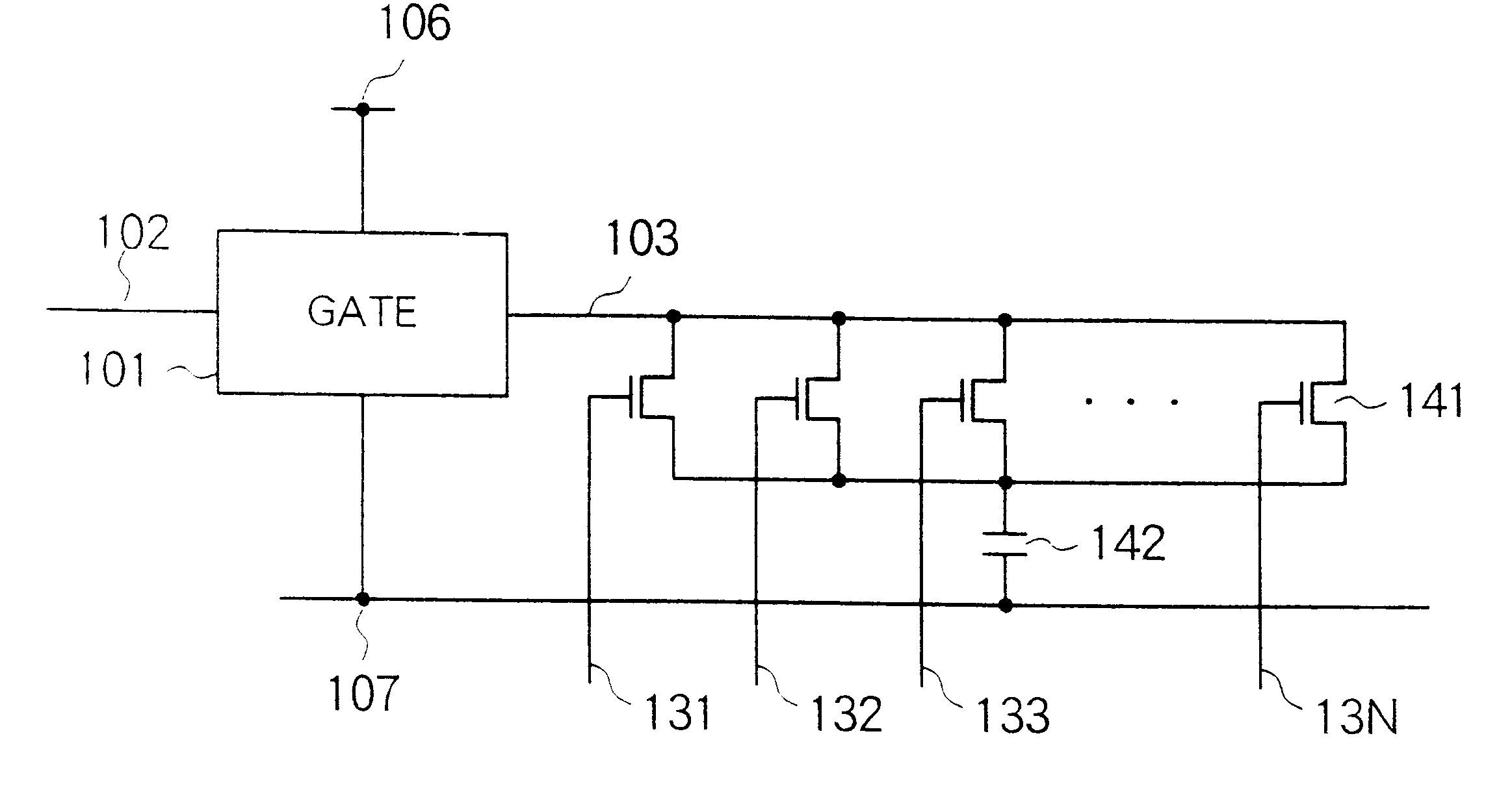
Referring to FIG. 6, a variable delay circuit according to the present invention comprises a gate element 101, which is similar to that shown in FIG. 4, connected between source lines 106 and 107 and having an input 102 and an output 103, and a plurality (N) of parallel nMOSFETs 141 connected in series with a capacitor 142 between the output line 103 of the gate element 101 and the low potential source line 107.

Specifically, the combination of the plurality of MOSFETs 141 and the capacitor 142 constitutes an RC network, wherein the resistance R is controlled by a set of control signals supplied to the gate electrodes 131 to 13N of the nMOSFETs 141. The capacitance of the capacitor 142 is preferably set between 100 fF and 500 fF for a set of L / W's for the nMOSFETs 141 similar to those of the first embodiment.

In FIG. 6, assuming that the total ON-current of nMOSFETs 141 which are ON due to a specific set of control signals is expressed by "I", the delay is in proportion to 1 / I. By emp...

third embodiment

Referring to FIG. 7, a variable delay circuit according to the present invention comprises a plurality (M) of cascaded delay sections 161 each implemented by a variable delay circuit of FIG. 3. Each delay section 161 is controlled by a common set of control signals supplied through control lines 111 to 11N and 121 to 12N of the each delay section 161. The variable delay circuit of FIG. 7 achieves a wider control range for the delay time which is M times the control range of the variable delay circuit of FIG. 3.


PUM


Abstract

A variable delay section comprises a gate element and a plurality of (N) delay elements for delaying the signal change on the output of the gate element. A difference between a first delay provided by n-th delay section and a second delay provided by (n+1)th delay section is constant for any of n's between 1 and N-1. A plurality of variable delay sections are cascaded to form a frequency multiplier, with the output of the last stage variable delay section being fed-back to the input of the first stage variable delay section through a selector. The other input of the selector is connected to the input of the variable delay circuit to allow the internal signal to pass the variable delay sections for K times.

Description

(a) Field of the InventionThe present invention relates to a variable delay circuit and, more particularly, to a variable delay circuit for providing a variable delay time capable of being controlled by a set of control signals.(b) Description of the Related ArtA variety of variable delay circuits have been proposed each providing a variable delay time capable of being controlled by a set of control signals supplied from outside the circuit. Since the variable delay circuit can be designed to implement a voltage controlled oscillator by connecting the output of the variable delay circuit with the input thereof for a negative feedback loop, it is sometimes described as a programmable voltage controlled oscillator.U.S. Pat. No. 4,978,927 to Hausman et al. discloses a programmable voltage controlled oscillator shown in FIG. 1. The voltage controlled oscillator has three basic gate circuits 202, 204 and 206, a first gate circuit 232 and a second gate circuit 226, all of which are connec...

Claims


Application Information

Patent Timeline
Patent Type & Authority Patents(United States)
IPC IPC(8): H03K5/13H03K5/00H03K3/03H03K3/00H03K5/131
CPCH03K5/131H03K3/0315H03K2005/00065H03K2005/00071
Inventor MIZUNO, MASAYUKI
Owner NEC CORP
Why Eureka
Try Eureka