SOI CMOS body contact through gate, self-aligned to source- drain diffusions

a body contact and diffusion technology, applied in the field of semiconductor devices, can solve the problems of limiting the effectiveness of body-charge equilibrium at high-speed, unstable device behavior, and degrading the ability of the device to remove by increasing the resistan

Inactive Publication Date: 2001-11-20
GLOBALFOUNDRIES INC
View PDF1 Cites 72 Cited by
  • Summary
  • Abstract
  • Description
  • Claims
  • Application Information

AI Technical Summary

Benefits of technology

FIG. 11 is an elevational view of the SOI structure of the present invention after deposition of a low-resistance region in the body-cont...

Problems solved by technology

In the silicon on insulator ("SOI") art, it is well recognized that the resistance-capacitance ("RC") delay associated with body-contacts to wide channel MOSFETS limits the effectiveness of body-charge equilibrium at high-speeds.
The resistance of the path increases with increasing width of the main channel until RC time constant of the body contact becomes a significant factor, which may cause unstable de...

Method used


Image

  • SOI CMOS body contact through gate, self-aligned to source- drain diffusions
  • SOI CMOS body contact through gate, self-aligned to source- drain diffusions
  • SOI CMOS body contact through gate, self-aligned to source- drain diffusions

Examples


Embodiment Construction

)

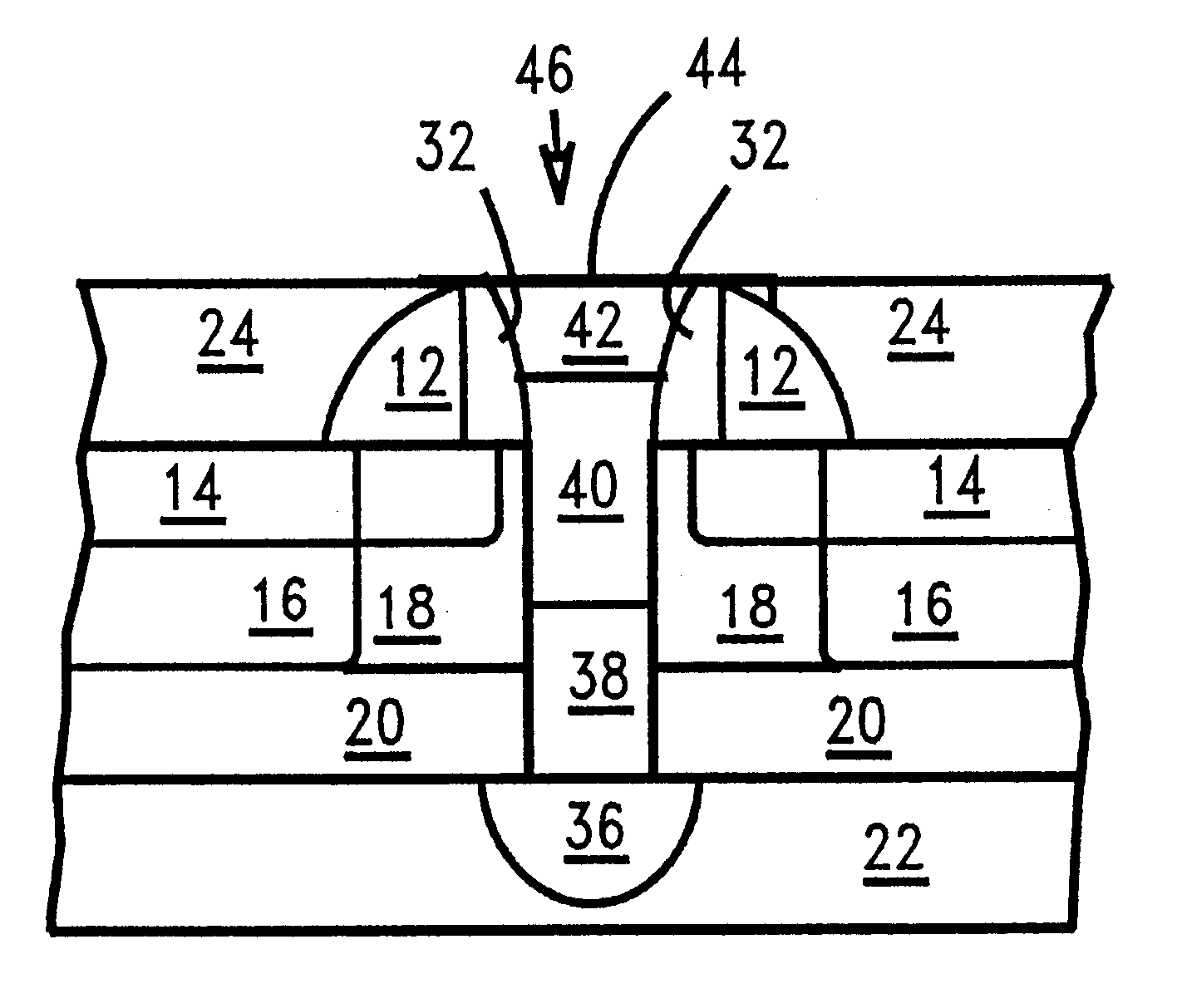
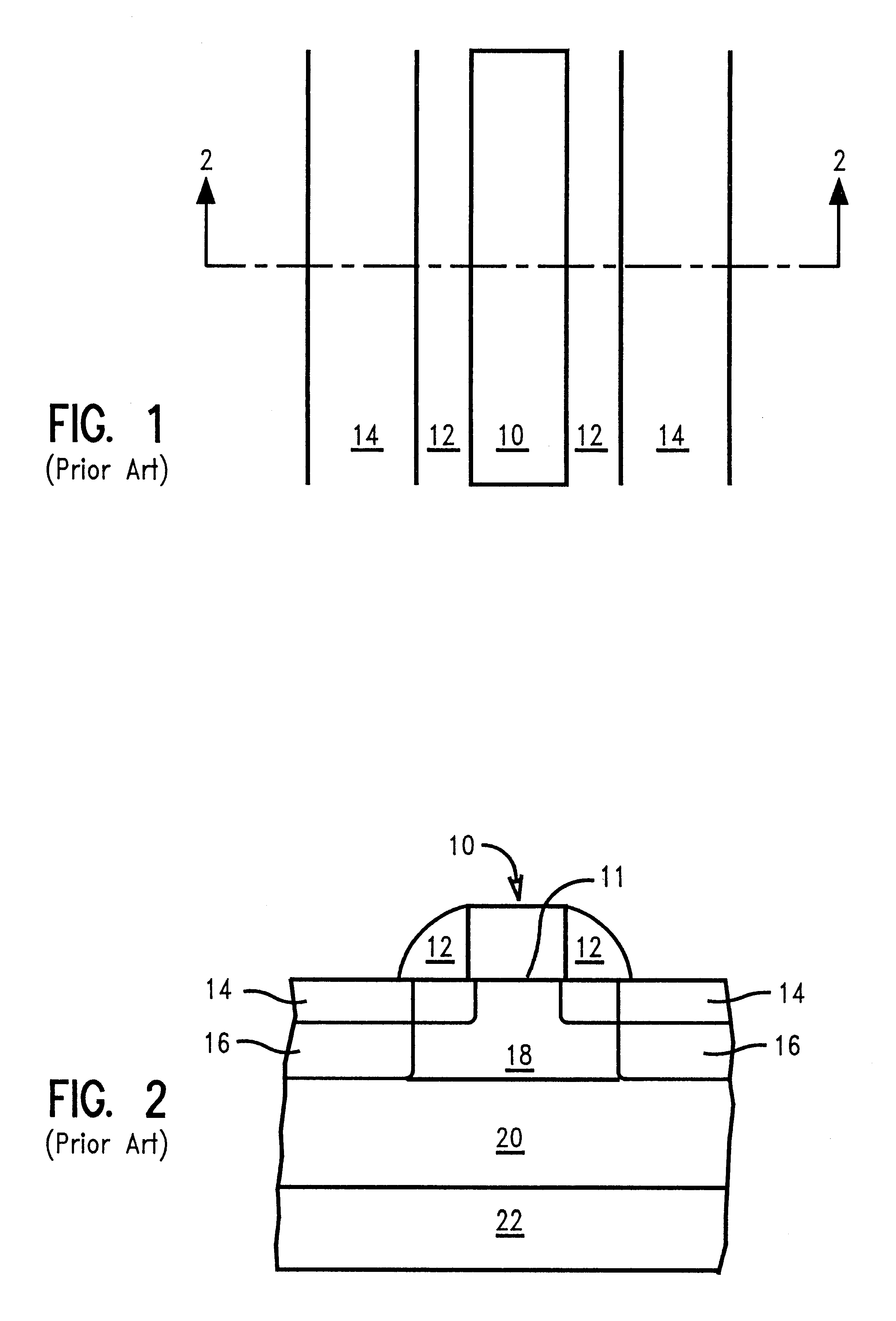
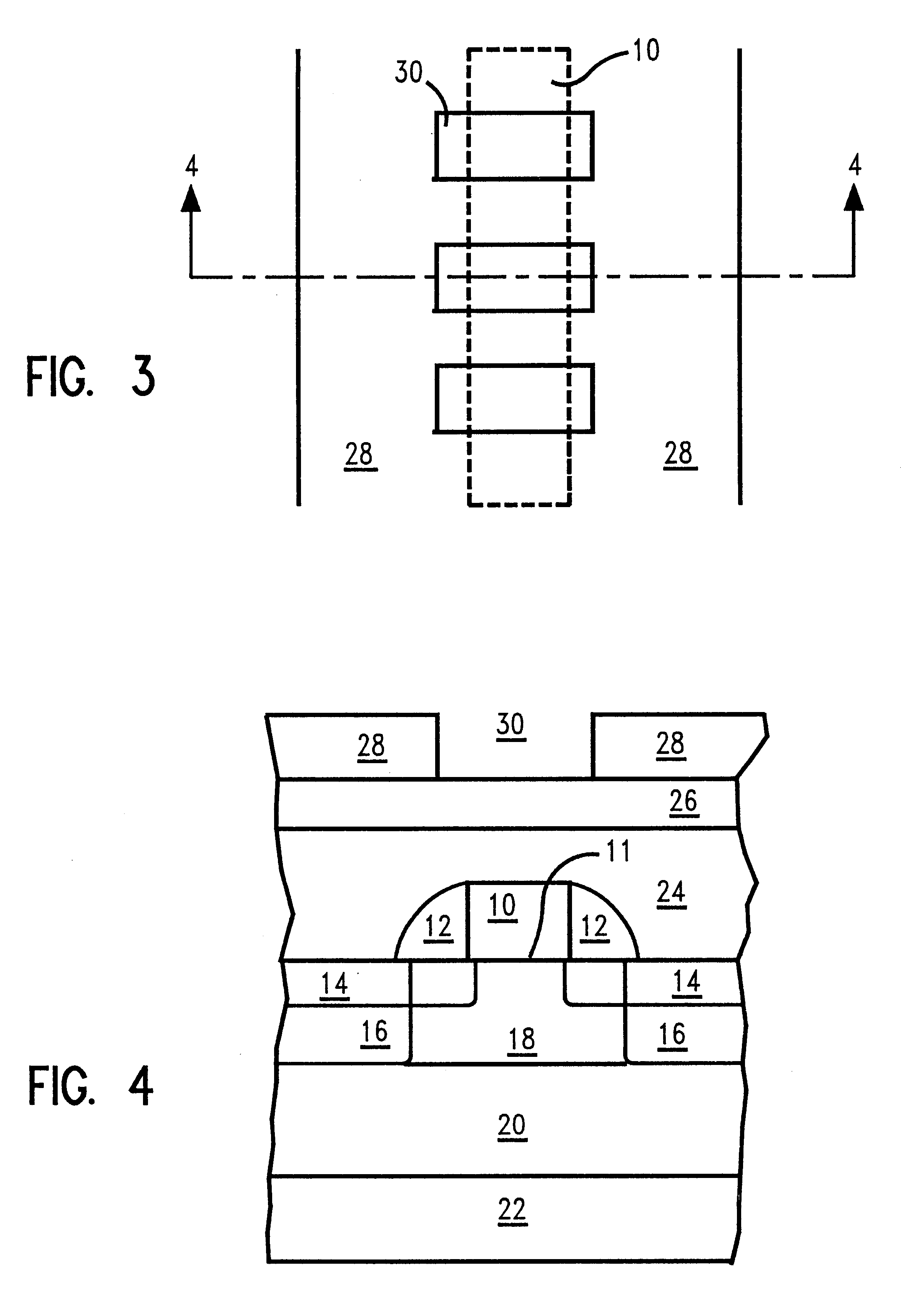
In describing the preferred embodiment of the present invention, reference will be made herein to FIGS. 1-13 of the drawings in which like numerals refer to like features of the invention. Features of the invention are not necessarily shown to scale in the drawings. As used herein, unless otherwise noted, the terms "insulating" or "insulator" means "electrically insulating" and the term "contact" mean "electrical contact." The terms "on top of" or "over" are also used to denote "electrical contact."

The present invention creates a semiconductor device with SOI body-contacts under the gate conductor. The body-contacts are self aligned and borderless to adjacent source / drain diffusions, thus preventing diffusion-to-body shorts. In the typical MOSFET device, the body charge must traverse along the width direction of the transistor with a relatively long path. The present invention partitions the gate conductor into segments and provides body-contacts under each gate conductor segment o...


PUM


Abstract

A structure and process for making a semiconductor device with SOI body contacts under the gate conductor. The gate conductor is partitioned into segments and provides a body contact under each gate conductor segment over the width of the device. A plurality of body contacts may be distributed across the length of the gate conductor. This results in a relatively short path for holes leaving the body to traverse and allows accumulated charge to be removed from the body region under the gate. The structure provides for stable and efficient body-contact operation for SOI MOSFETS of any width operating at high speeds.

Description

1. Field of the InventionThe present invention relates generally to a semiconductor device, and more particularly to a method for forming a silicon on insulator structured substrate with body-contacts under the gate conductor.2. Description of Related ArtIn the silicon on insulator ("SOI") art, it is well recognized that the resistance-capacitance ("RC") delay associated with body-contacts to wide channel MOSFETS limits the effectiveness of body-charge equilibrium at high-speeds. This occurs because the charge associated with the SOI body must traverse the half-width of the MOSFET. The resistance of the path increases with increasing width of the main channel until RC time constant of the body contact becomes a significant factor, which may cause unstable device behavior. The increased resistance degrades the ability of the device to remove hole charge (majority carriers in an NMOSFET) because in a wide channel device the holes leaving the body must traverse a long path. An analogou...

Claims


Application Information

Patent Timeline
IPC IPC(8): H01L27/12H01L21/28H01L21/768H01L23/522H01L29/78H01L29/786
CPCH01L27/1203H01L2924/0002H01L2924/00H01L21/743H01L21/76831H01L21/76897H01L29/78
Inventor HARGROVE, MICHAEL J.MANDELMAN, JACK A.
Owner GLOBALFOUNDRIES INC
Why Eureka
Try Eureka