Non-volatile memory device with single-layered overwriting transistor

a memory device and transistor technology, applied in semiconductor devices, instruments, electrical devices, etc., can solve the problems of low product reliability, failure to form a channel in order to stop current, and memory cells constructed in the above manner will have problems in the overwriting process

Inactive Publication Date: 2001-11-27
SAMSUNG ELECTRONICS CO LTD
View PDF10 Cites 16 Cited by
  • Summary
  • Abstract
  • Description
  • Claims
  • Application Information

AI Technical Summary

Problems solved by technology

The disadvantage of the one transistor cell is that it exhibits low product reliability when compared with the two transistor cell, i.e., the FLOTOX type of cell.
If a supply voltage is applied to the select gate, the control gate and the bit line, in order to read the cell, the higher threshold voltage Vth results in a failure to form a channel in order to stop the current from flowing.
However, in accordance to the prior art, an EEPROM device having a memory cell being constructed in the above manner will have problems in the overwriting process.
That is, problems in the process of performing another programming process to erased the "off state" of a cell and to memorize another data input after a programming process is performed.
In this case a current path is formed through source (S) and cell 1, which become the common grounding line, thereby cause a programming failure of the programming process for cell 5.
However, if the overwriting process is performed in this programming method, there may be operational failures in the EEPROM device as it is now operating in a mode different from the programming process desired by a programmer.
Therefore, the aforementioned programming method of the EEPROM device can not be used effectively.

Method used


Image

  • Non-volatile memory device with single-layered overwriting transistor
  • Non-volatile memory device with single-layered overwriting transistor
  • Non-volatile memory device with single-layered overwriting transistor

Examples


Embodiment Construction

Applicants' Korean Patent Application No. 99-28217, filed Jul. 13, 1999 is incorporated herein by reference as if fully set forth herein.

Hereinafter, a preferred embodiment of the present invention will be described in detail with reference to the accompanying drawings.

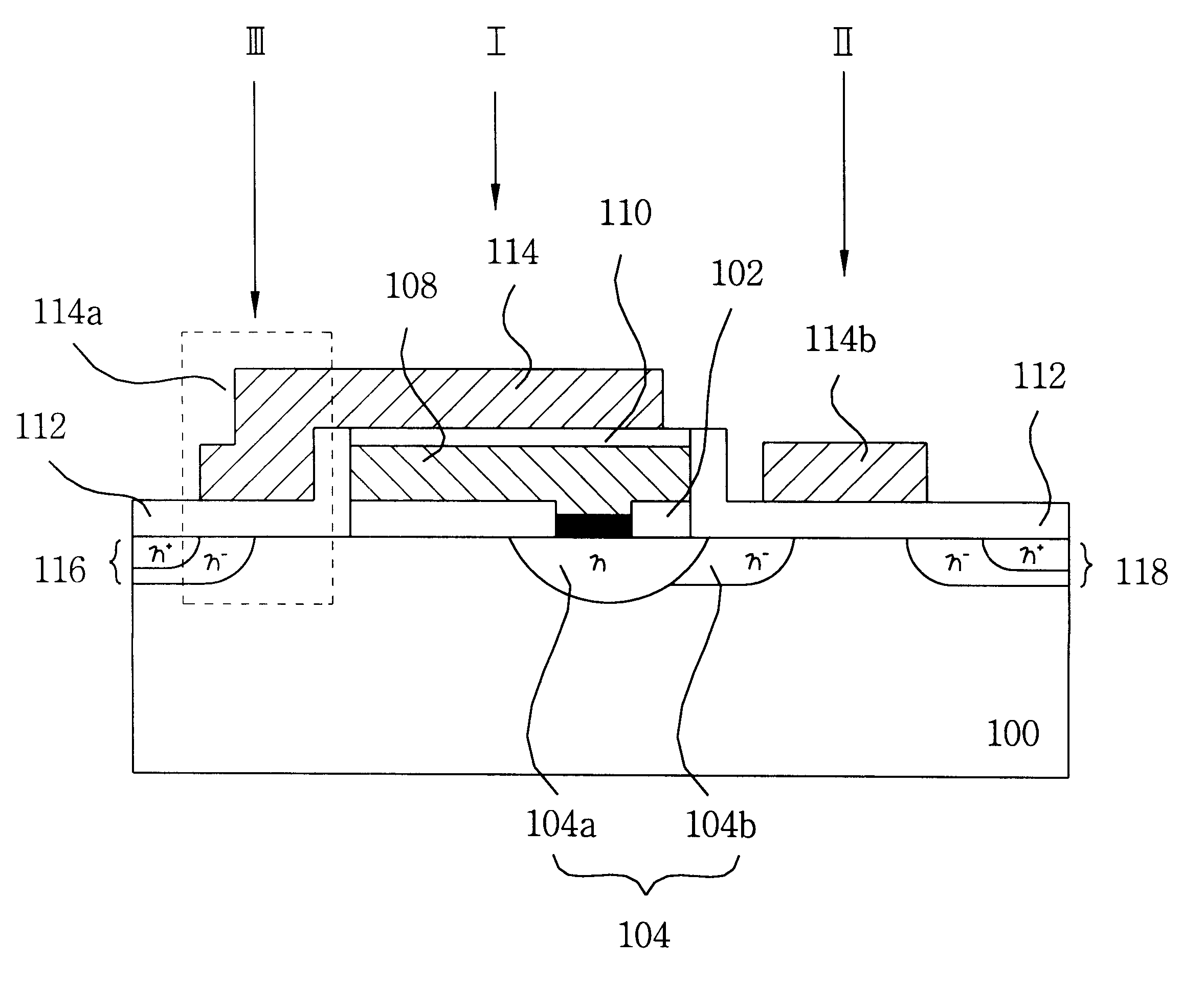
Referring to FIGS. 4 and 5, a FLOTOX type EEPROM device comprises a n-type junction 104 formed at a predetermined position inside a p-type substrate 100. A source 116, constructed in an n- / n+ double junction structure inside the substrate 100, is at a predetermined distance from one side of the junction 104. A drain 118, constructed in an n- / n+ double junction structure inside the substrate 100, is at a predetermined distance from the other side of the junction 104. A sense transistor I includes a gate formed in a deposition structure of a first conductivity layer 108, an interlevel insulating layer 110 and a second conductivity layer 114, and partially overlaps the junction 104. The sense transistor I also includes a...


PUM


Abstract

A non-volatile memory device that can prevent a functional failure in the programming process of a cell from occurring in an overwriting process, by stopping a current path from being formed through the sources of a previously programmed cell and that of a currently selected cell which is to be programmed. The present device includes a modified structure for a memory cell of an EEPROM device. The present device includes an additional overwrite transistor to separate a sense transistor from a source in the region of an active area which is expanded toward the source of the sense transistor. The overwriting transistor includes a gate formed in a single layered structure of a second conductivity layer, integrally connected with the second conductivity layer of the sense transistor. Further, a second gate insulating layer is formed between the source and the sense transistor on the substrate. Accordingly, an electric path is prevented from forming through sources of the previously programmed cell and that of the selected cell to be programmed and, in turn, to prevent the overwriting process from having any programming failure.

Description

1. Field of the InventionThe present invention relates to a non-volatile memory device and, more particularly, to a non-volatile memory device which can prevent a program failure from occurring in an overwriting process of an electrically erasable programmable read only memory (EEPROM).2. Brief Description of the Background ArtDifferent from SRAM or DRAM, an electrically erasable programmable read only memory (EEPROM) cell is a non-volatile memory cell useful for electrically erasing, storing and maintaining data without a power supply. Recently, EEPROM cells have been utilized in a variety of applications.An EEPROM cell is classified as either a flash type memory device comprising a single cell with one transistor or a floating gate tunnel oxide type (FLOTOX) device comprising a single cell with two transistors. The former type of cell, constructed with one transistor, has an advantage in that a unit cell has a small size. The disadvantage of the one transistor cell is that it exhi...

Claims


Application Information

Patent Timeline
Patent Type & Authority Patents(United States)
IPC IPC(8): H01L29/66H01L29/40H01L29/423H01L29/788G11C16/00
CPCH01L29/42324H01L29/7883G11C16/00
Inventor PARK, WEON-HOHAN, JEONG-UK
Owner SAMSUNG ELECTRONICS CO LTD
Why Eureka
Try Eureka