Hybrid wiring board, semiconductor apparatus, flexible substrate, and fabrication method of hybrid wiring board

a technology of hybrid wiring and flexible substrate, which is applied in the field of hybrid wiring board, can solve the problems of difficult to form a finer wiring pattern, restricted thickness of build-up board, and inconvenient wire bonding technology and tab (tape automated bonding) technology cannot meet such requirements

Inactive Publication Date: 2001-12-11
KK TOSHIBA
View PDF16 Cites 223 Cited by
  • Summary
  • Abstract
  • Description
  • Claims
  • Application Information

AI Technical Summary

Problems solved by technology

However, conventional wire bonding technologies and TAB (Tape Automated Bonding) technologies cannot satisfy such requirements.
Thus, it is very difficult to form a finer wiring pattern than the uneven surface.
In addition, the thickness of the build-up board is restricted.
However, when the thickness of the core layer is decreased, the reliability of the resultant semiconductor package deteriorates.
In addition, it is difficult to form the build-up layers.
When the thickness of the build-up layers is decreased, it is difficult to form a wiring pattern at fine pitches.
Thus, practically, it is very difficult to decrease the thickness of the build-up board to 0.8 mm or less.
However, when through-holes are formed in a wiring board by a drill or the like, the glass fibers are broken as well as the insulation resin.
In this case, the conductive substance that permeates the separate portions deteriorates the insulation between the through-holes.
Thus, it is very difficult to mount a semiconductor device with connection terminals disposed at very fine pitches on a build-up board.
In addition, to structure such a semiconductor device as a semiconductor package, it is difficult to use a build-up board.
However, in such a layer connecting method, it takes a time to form the bumps.
In addition, it takes a time to form a metal layer (pad) to be bonded to the bumps.
Thus, in this method, the yield is low and thereby the fabrication cost is high.
In this case, when the solder is melted and connected to the wiring layers, the solder may adversely spread out.
Thus, this method is not suitable for fine connections.
Thus, sufficient connecting reliability cannot be obtained.
When such a load cumulates in the solder balls, they crack and thereby the connecting reliability largely

Method used


Image

  • Hybrid wiring board, semiconductor apparatus, flexible substrate, and fabrication method of hybrid wiring board
  • Hybrid wiring board, semiconductor apparatus, flexible substrate, and fabrication method of hybrid wiring board
  • Hybrid wiring board, semiconductor apparatus, flexible substrate, and fabrication method of hybrid wiring board

Examples


first embodiment

(First Embodiment)

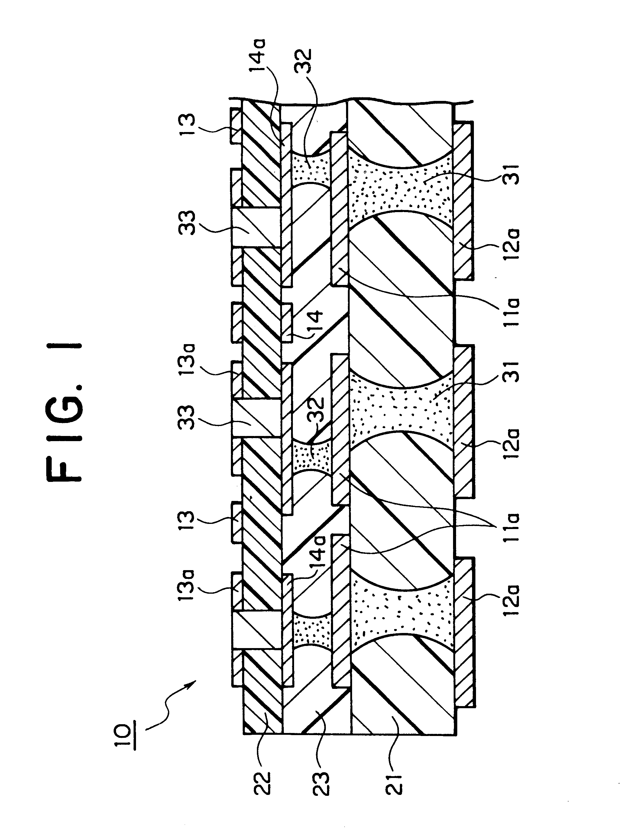
FIG. 1 is a sectional view showing the structure of a hybrid wiring board according to a first embodiment of the present invention.

Referring to FIG. 1, a hybrid wiring board 10 is a laminate wiring board having four wiring layers 11, 12, 13, and 14. The wiring layer 11 and the wiring layer 12 are insulated with a first insulation layer 21 that is a rigid layer. The wiring layer 13 and the wiring layer 14 are insulated with an insulation layer 22 that is a flexible layer. The wiring layer 11 and the wiring layer 14 are insulated with a third insulation layer 23 that is more rigid than the second insulation layer 22. The wiring layers 11, 12, 13, and 14 have land portions 11a, 12a, 13a, and 14a as parts of their wiring patterns, respectively.

The wiring layers 11, 12, 13, and 14 are formed by patterning conductive metal foil such as copper foil.

The first insulation layer 21 is made of prepreg of which a glass cloth is impregnated with BT resin. The second insulation l...

second embodiment

(Second Embodiment)

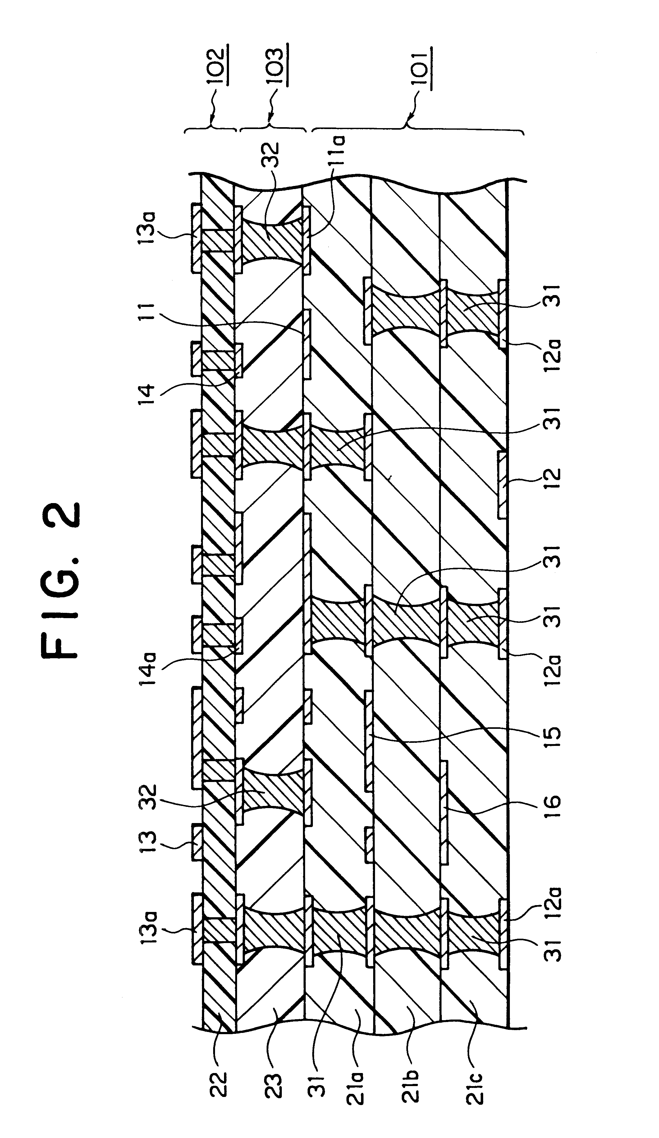
In the hybrid wiring board shown in FIG. 1, the structure of which the rigid substrate made of the first insulation layer 21 (rigid layer) and the wiring layers 11 and 12 disposed on both the surfaces thereof and the flexible substrate made of the second insulation layer 22 (flexible layer) and the wiring layers 13 and 14 disposed on both the surfaces thereof are electrically and mechanically connected with the third insulation layer 23 and the conductive pillar 32 was exemplified. However, the present invention is not limited to such a structure. Instead, as the rigid substrate and the flexible substrate connected to the third insulation layer, substrates having three or more wiring layers may be used.

FIG. 2 is a sectional view showing the structure of a hybrid wiring board according to a second embodiment of the present invention. In the hybrid wiring board shown in FIG. 2, a rigid substrate 101 is a laminate of four wiring layers 11, 12, 15, and 16 and three in...

third embodiment

(Third Embodiment)

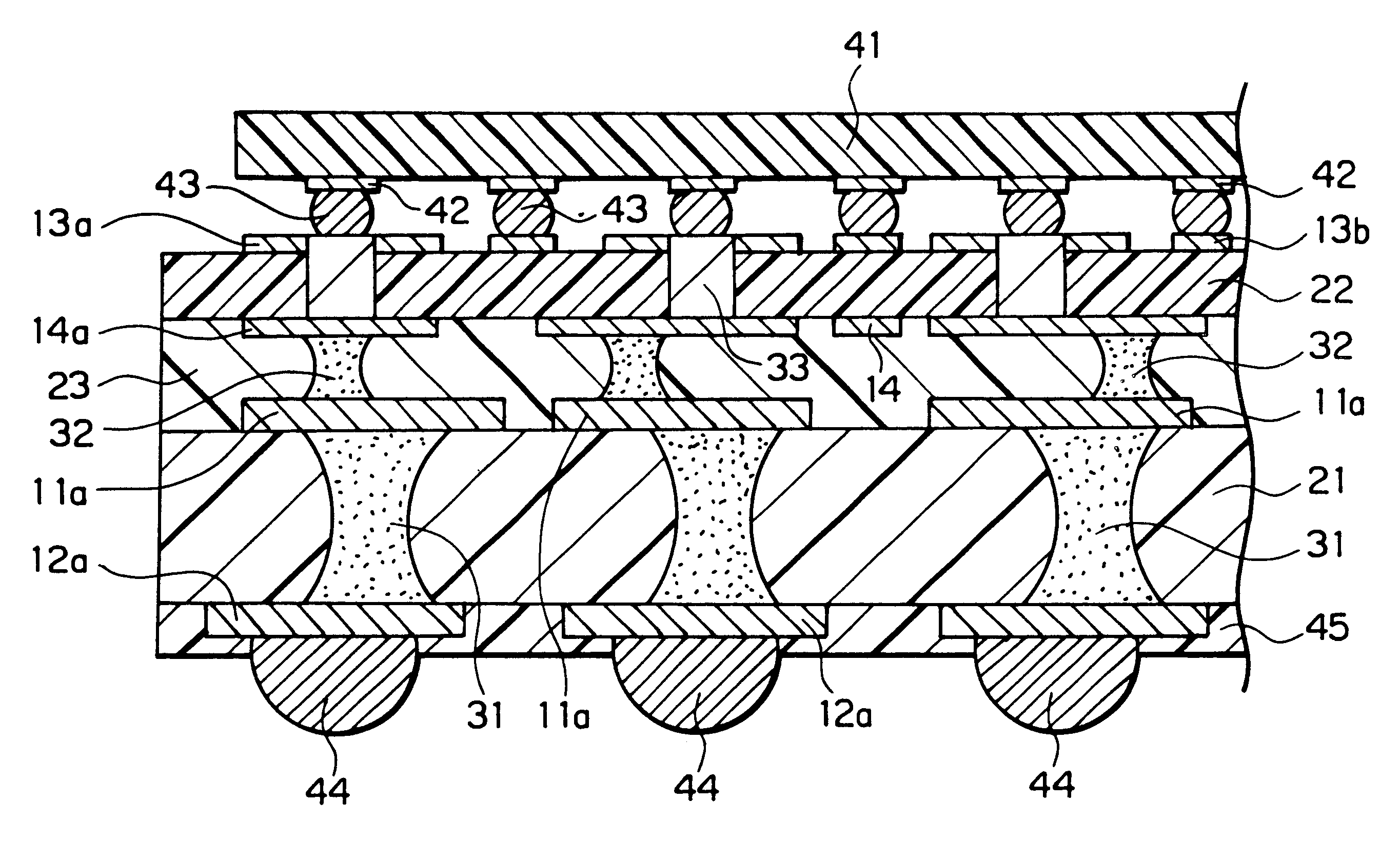
FIG. 3 is a sectional view showing the structure of a semiconductor package according to a third embodiment of the present invention.

The semiconductor package shown in FIG. 3 is a BGA package of which a semiconductor device 41 is mounted on the hybrid wiring board 10 shown in FIG. 10 according to the present invention by flip-chip bonding method.

The semiconductor device 41 is a bare chip. The semiconductor device 41 has a connecting pad 42 connected to an integrated circuit disposed in the semiconductor device. In this example, 900 connecting pads 42 are disposed on the lower surface of the semiconductor device 41 at pitches of around 0.35 mm in a full grid pattern.

A wiring layer 13 disposed on a second insulation layer 22 (flexible layer) of the hybrid wiring board has a connecting pad 13b or a via land 13a corresponding to the connecting pad 42 of the semiconductor device 41.

The connecting pad 13b or the via land 13a is bonded to the connecting pad 42 of the semi...


PUM


Abstract

A first via land of a wiring layer on a first surface of a first insulation layer that is a rigid layer and a second via land of a wiring layer on a second surface of a second insulation layer that is a flexible layer are electrically and mechanically connected with a conductive pillar pierced through a third insulation layer disposed between the first insulation layer and the second insulation layer. In such a structure, a wiring board that can mount a highly integrated semiconductor device, that is small and thin, and that has high reliability can be accomplished.

Description

1. Field of the InventionThe present invention relates to a wiring board such as a printed wiring board, in particular, to a hybrid wiring board that is a combination of a rigid wiring substrate and a flexible wiring substrate.In addition, the present invention relates to a flexible wiring substrate of which a wiring layer is disposed on insulation resin film, in particular, to a flexible wiring substrate laminated with a rigid wiring substrate.Furthermore, the present invention relates to a semiconductor apparatus such as a semiconductor package of which a semiconductor device is mounted on a printed wiring board, in particular, to a semiconductor apparatus that mounts a semiconductor device with connection terminals disposed at a high mounting density.Moreover, the present invention relates to a fabrication method of a printed wiring board, in particular, to a fabrication method of a hybrid wiring board that is a combination of a rigid wiring substrate and a flexible wiring substr...

Claims


Application Information

Patent Timeline
IPC IPC(8): H01L23/498H01L23/48H05K3/46H05K3/40H01L23/12
CPCH01L23/49827H01L23/49833H05K3/462H01L2224/16H01L2924/0102H01L2924/01078H01L2924/01079H01L2924/15311H05K3/4069H05K3/4647H05K3/4688H05K2201/096H05K2203/1189H01L2924/01019H01L2924/01087H01L2924/01322H05K3/4691H01L2224/16225H01L2224/16235H05K2201/068H01L2224/05573H01L2224/05568H01L2924/00014H01L2224/05599H05K1/116H05K3/3436
Inventor TAKUBO, CHIAKISATO, YOSHIZUMIKOJIMA, TOMITSUGUTAKEDA, GO
Owner KK TOSHIBA
Why Eureka
Try Eureka