Semiconductor integrated circuit device

a technology of integrated circuit devices and semiconductors, applied in the direction of memory adressing/allocation/relocation, digital storage, instruments, etc., can solve the problems of increasing the speed of drams that cannot meet the high-speed performance of mpus, the speed of increasing drams is relatively slow and the cost of manufacture is relatively low,

Inactive Publication Date: 2002-01-01
RENESAS ELECTRONICS CORP
View PDF13 Cites 40 Cited by
  • Summary
  • Abstract
  • Description
  • Claims
  • Application Information

AI Technical Summary

Problems solved by technology

In general, computer systems use semiconductor devices of large capacities, in which processing speeds are relatively slow and costs in manufacture are relatively low, as main storage devices.
However, increasing the speeds of the DRAMs do not sufficiently catch up with the high-speed performance of the MPUs.
The aforementioned related arts suffer from drawbacks such as operational delays in data transfer due to cache mishit events, for example.
However, the aforementioned techniques are disadvantageous in that an area of the bidirectional data transfer circuit is large enough to occupy an overall area of the semiconductor substrate.
So, there is a limit in a number of the circuits being installed on the semiconductor substrate.
As a result, there is a limit in a number of transfer bus lines being provided with respect to the semiconductor storage device.
Such a memory system of FIG. 46 suffers from a drawback in which a cache hit rate is reduced upon receipt of access requests from the multiple processing devices.
If a CD-RAM or ED-RAM (where "ED" stands for "Exchangeable Disk") is used as a main memory (9115) shown in FIG. 46, the cache hit rat...

Method used


Image

  • Semiconductor integrated circuit device
  • Semiconductor integrated circuit device
  • Semiconductor integrated circuit device

Examples


Embodiment Construction

of Circuit Blocks

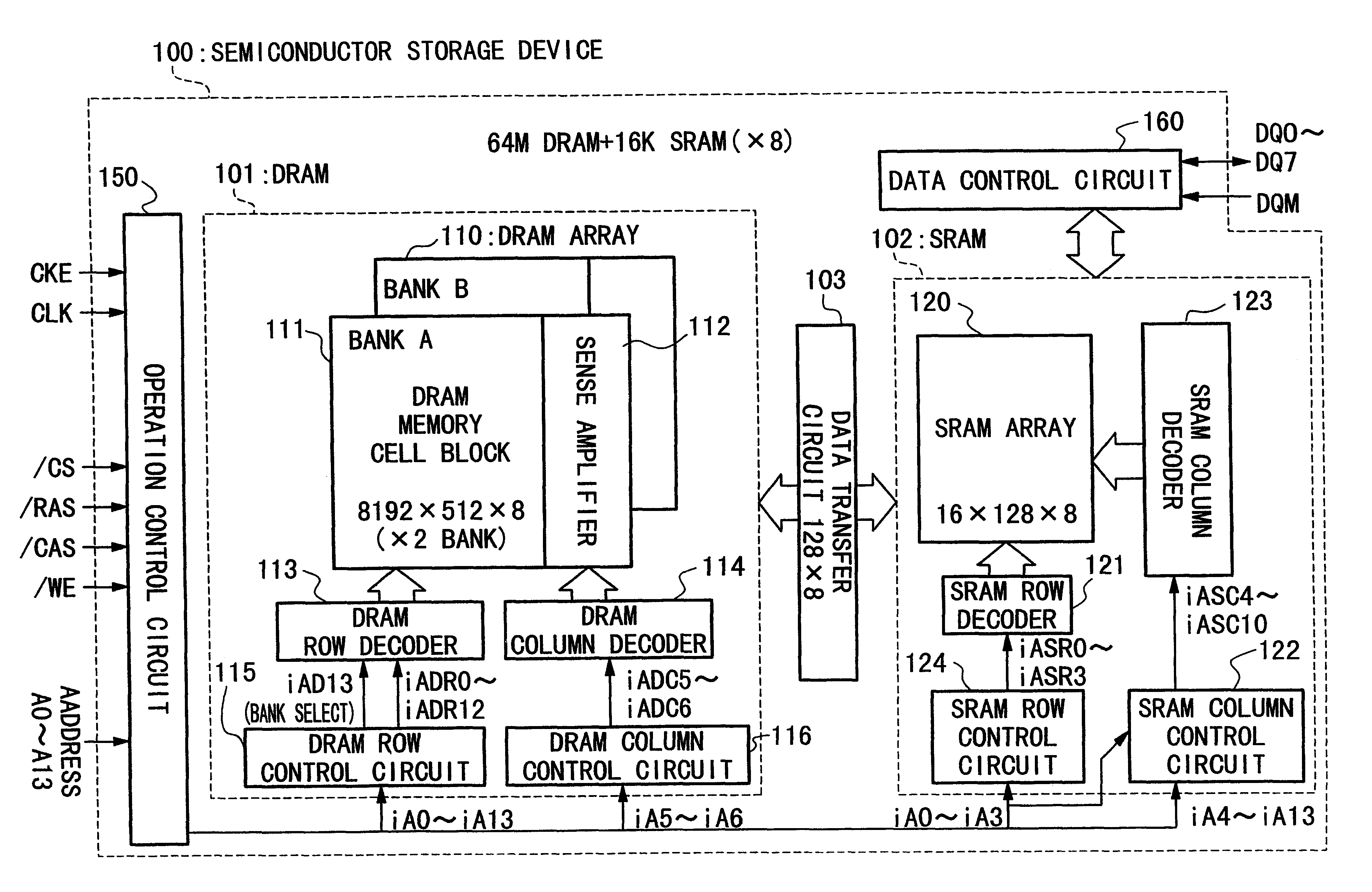
Next, detailed descriptions will be given with respect to circuit blocks shown in the block diagram of FIG. 1.

The following descriptions merely show examples, so this invention is not necessarily limited to those examples.

1. Operation Control Circuit

FIG. 27 is a block diagram showing an internal configuration of the operation control circuit 150 shown in FIG. 1. The operation control circuit 150 is basically configured by an internal clock generation circuit 410, a command decoder 420, a control logic 430, an address control circuit 440 and a mode register 450. The internal clock generation circuit 410 generates an internal clock signal iCLK based on the clock signal CLK and clock enable signal CKE which are given from the external. The internal clock signal iCLK is delivered to the command decoder 420, control logic 430, address control circuit 440 and other data control circuits so as to perform timing controls on them.

The command decoder 420 contains an input buf...


PUM


Abstract

A semiconductor integrated circuit device is configured using a DRAM and an SRAM between which data transfer is performed by way of a data transfer circuit using data transfer bus lines. Herein, the DRAM is divided into at least two DRAM arrays, each of which contains a number of columns each consisting of memory cells. In addition, the columns are arranged in mixture in connection with external I/O terminals respectively in such a way that columns respectively containing memory cells which are simultaneously subjected to read operations within a same cycle are arranged not to adjoin each other. Thus, it is possible to reduce a probability in which multiple memory cells which are simultaneously subjected to read operations within the same cycle exist within a range of an area under influence of charged particles, which are produced locally due to neutrons. Even if data of memory cells which are concentrated at a certain region are simultaneously placed under influence of the charged particles, it is possible to remarkably reduce a number of chances in that multiple bits of data being read out to the external I/O terminals go defective simultaneously.

Description

1. Field of the InventionThis invention relates to semiconductor integrated circuit devices having plenty of external I / O terminals for inputting and outputting data, and particularly to semiconductor integrated circuit devices in which data transfer circuits are provided between main storages and auxiliary storages being formed on same semiconductor substrates.This application is based on Patent Application No. Hei 11-69308 filed in Japan, the content of which is incorporated herein by reference.2. Description of the Related ArtIn general, computer systems use semiconductor devices of large capacities, in which processing speeds are relatively slow and costs in manufacture are relatively low, as main storage devices. To suite requirements of the main storage devices, the computer systems frequently use general-purpose DRAMs (i.e., dynamic random-access memories).In the computer systems in these days, engineers develop DRAMs, which construct main storage portions, to increase proces...

Claims


Application Information

Patent Timeline
IPC IPC(8): G11C11/412G11C11/00G06F12/08G11C11/401G11C11/407G11C11/41G11C11/413H01L21/8242H01L27/108
CPCG11C11/4125G11C11/005G11C11/40
Inventor KAWAGUCHI, MASAKIFUJII, TAKEOMATSUI, YOSHINORIFURUTA, HIROSHIHANNAI, SEIICHI
Owner RENESAS ELECTRONICS CORP
Why Eureka
Try Eureka