Deliberate semiconductor film variation to compensate for radial processing differences, determine optimal device characteristics, or produce small productions

a semiconductor film and radial processing technology, applied in the field of selective semiconductor film variation, can solve the problems of radial differences in device characteristics, less wafers, and less waste, and achieve the effect of reducing the radial effect of cmp

Inactive Publication Date: 2002-02-05
IBM CORP
View PDF20 Cites 13 Cited by
  • Summary
  • Abstract
  • Description
  • Claims
  • Application Information

AI Technical Summary

Benefits of technology

FIGS. 19 through 22 illustrate cross-sectional views of a semiconductor wafer during a preferred method, in accordance wit...

Problems solved by technology

Both of these radial processing effects will cause radial differences in device characteristics between devices formed at the center of the wafer and devices formed near the outer periphery of the wafer.
Additionally, as the semiconductor industry progresses towards very large wafer sizes, there will be more waste during the small batches that are used to determine optimal device characteristics.
However, these few wafers and the processing time and steps performed to complete them can be relatively expensive.
Moreover, as the semiconductor industry converts to large wafer sizes, small batches of specialty chips, especially those made for a small chip designer, can become relatively expensive.
During production ...

Method used


Image

  • Deliberate semiconductor film variation to compensate for radial processing differences, determine optimal device characteristics, or produce small productions
  • Deliberate semiconductor film variation to compensate for radial processing differences, determine optimal device characteristics, or produce small productions
  • Deliberate semiconductor film variation to compensate for radial processing differences, determine optimal device characteristics, or produce small productions

Examples


Embodiment Construction

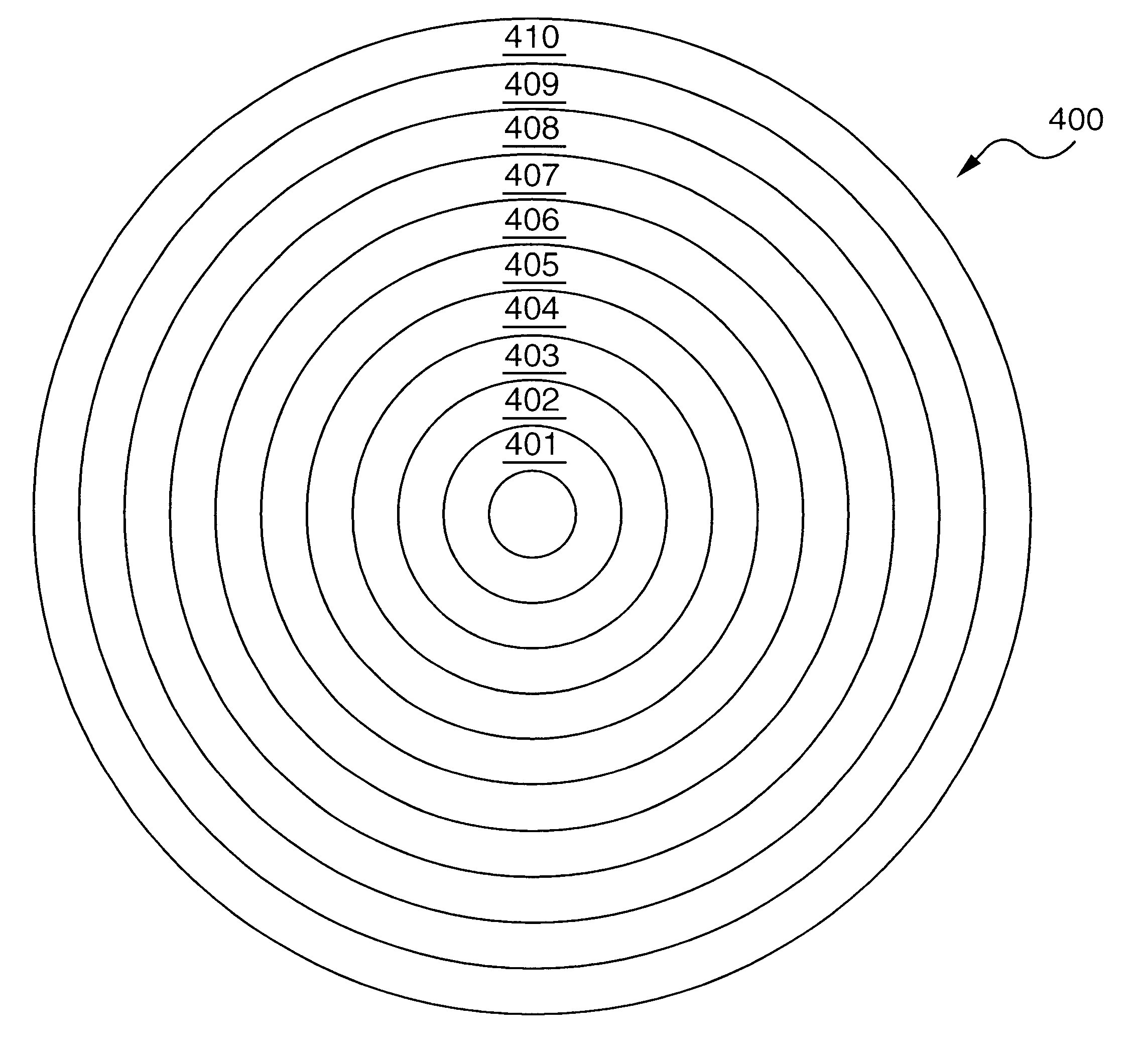
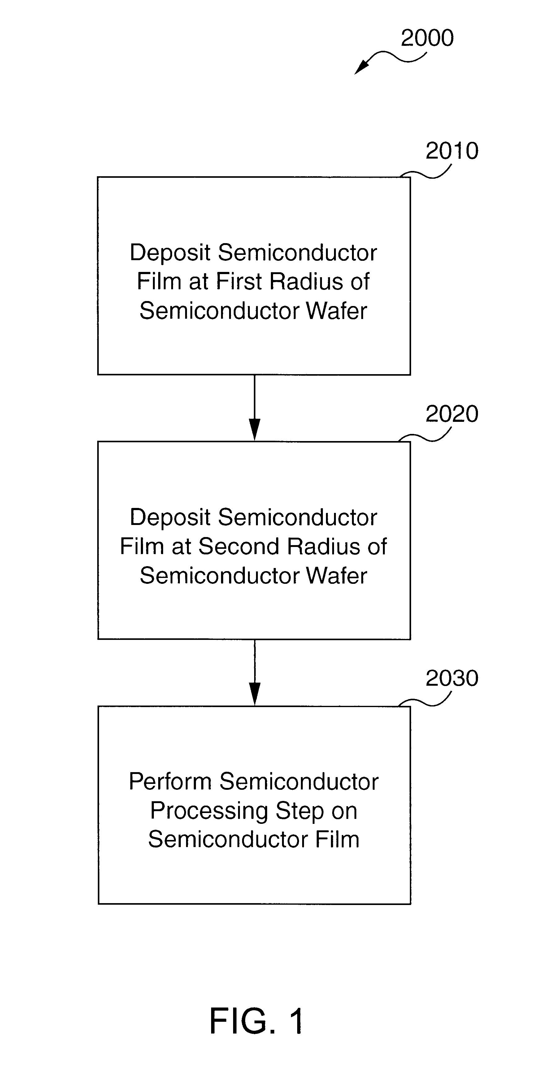
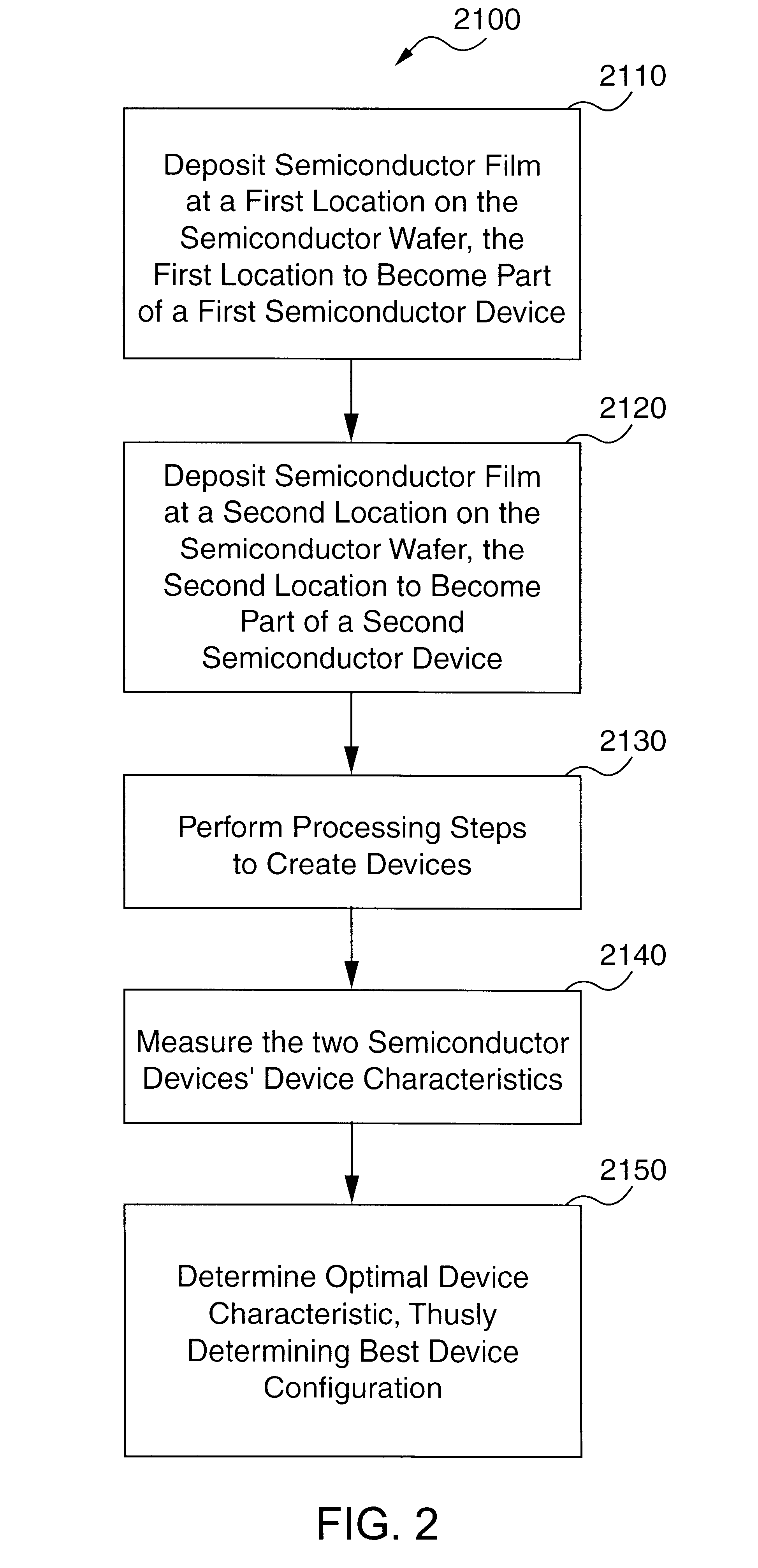
The preferred embodiments of the present invention overcome the limitations of the prior art and provide methods and apparatuses that can introduce deliberate semiconductor film variation during semiconductor manufacturing to compensate for radial processing differences or to determine optimal device characteristics. The present invention radially varies the thickness and / or composition of a semiconductor film to compensate for a known radial variation in the semiconductor film that is caused by performing a subsequent semiconductor processing step on the semiconductor film.

For example, it is known that a gate conductor stack will be etched more at the outer circumference of the semiconductor wafer than at an inner circumference of the semiconductor wafer. This causes wider gates at the inner circumference of the semiconductor wafer than at the outer circumference of the semiconductor wafer. Using the current invention, the thickness and / or composition of the gate conductor stack ma...


PUM

PropertyMeasurementUnit
Thicknessaaaaaaaaaa
Radiusaaaaaaaaaa
Semiconductor propertiesaaaaaaaaaa

Abstract

Methods and apparatuses are disclosed that can introduce deliberate semiconductor film variation during semiconductor manufacturing to compensate for radial processing differences, to determine optimal device characteristics, or produce small production runs. The present invention radially varies the thickness and/or composition of a semiconductor film to compensate for a known radial variation in the semiconductor film that is caused by performing a subsequent semiconductor processing step on the semiconductor film.Additionally, methods and apparatuses are disclosed that can introduce deliberate semiconductor film variations to determine optimal device characteristics or produce small production runs. Introducing semiconductor film variations, such as thickness variations and/or composition variations, allow different devices to be made. A number of devices may be made having variations in semiconductor film. Because the semiconductor film has variations between the devices, device characteristics of the devices should be different. By measuring the device characteristics of devices having the variations, the device with the optimum device characteristic may be chosen, thereby indicating the appropriate semiconductor film thickness and/or composition. Moreover, small production runs of the same devices, having different characteristics, will allow the end user to select the appropriate devices for their needs.

Description

1. Technical FieldThe present invention relates generally to the field of semiconductor manufacturing and, more specifically, to deliberate semiconductor film variation during semiconductor manufacturing to compensate for radial processing differences, determine optimal device characteristics, or produce small production runs.2. Background ArtSome semiconductor processing steps create radial differences across the wafer. For example, when performing Chemical-Mechanical Polishing (CMP) of the surface of a semiconductor wafer, the portion of the semiconductor wafer towards the outer circumference of wafer will be ground more than the inner portion of the semiconductor wafer. Similarly, during a Reactive Ion Etch (RIE) of the gate stack, the gates formed at the outer periphery of the semiconductor wafer will be etched more then the gates formed near the center of the semiconductor wafer. Consequently, the gates at the outer periphery of the semiconductor wafer will have a smaller width...

Claims


Application Information

Patent Timeline
IPC IPC(8): C23C16/04C23C16/52C23C16/50C23C16/513H01L21/762H01L21/70H01L21/8234H01L21/66H01L21/02H01L21/3213H01L21/3105H01L21/311
CPCC23C16/04C23C16/513C23C16/52H01L21/76229H01L21/8234H01L22/20H01L21/31053Y10S438/911H01L21/32137H01L21/31116
Inventor FURUKAWA, TOSHIHARUHAKEY, MARK C.HOLMES, STEVEN J.HORAK, DAVID V.
Owner IBM CORP
Why Eureka
Try Eureka